|
|
|
PDF AD9251 Data sheet ( Hoja de datos )
| Número de pieza | AD9251 | |
| Descripción | 1.8 V Dual Analog-to-Digital Converter | |
| Fabricantes | Analog Devices | |
| Logotipo | ||
Hay una vista previa y un enlace de descarga de AD9251 (archivo pdf) en la parte inferior de esta página. Total 30 Páginas | ||
|
No Preview Available !
Data Sheet
14-Bit, 20 MSPS/40 MSPS/65 MSPS/80 MSPS,
1.8 V Dual Analog-to-Digital Converter
AD9251
FEATURES
1.8 V analog supply operation
1.8 V to 3.3 V output supply
SNR
74.3 dBFS at 9.7 MHz input
71.5 dBFS at 200 MHz input
SFDR
93 dBc at 9.7 MHz input
80 dBc at 200 MHz input
Low power
33 mW per channel at 20 MSPS
73 mW per channel at 80 MSPS
Differential input with 700 MHz bandwidth
On-chip voltage reference and sample-and-hold circuit
2 V p-p differential analog input
DNL = ±0.45 LSB
Serial port control options
Offset binary, gray code, or twos complement data format
Optional clock duty cycle stabilizer
Integer 1-to-8 input clock divider
Data output multiplex option
Built-in selectable digital test pattern generation
Energy-saving power-down modes
Data clock out with programmable clock and data
alignment
APPLICATIONS
Communications
Diversity radio systems
Multimode digital receivers
GSM, EDGE, W-CDMA, LTE, CDMA2000, WiMAX, TD-SCDMA
I/Q demodulation systems
Smart antenna systems
Battery-powered instruments
Hand held scope meters
Portable medical imaging
Ultrasound
Radar/LIDAR
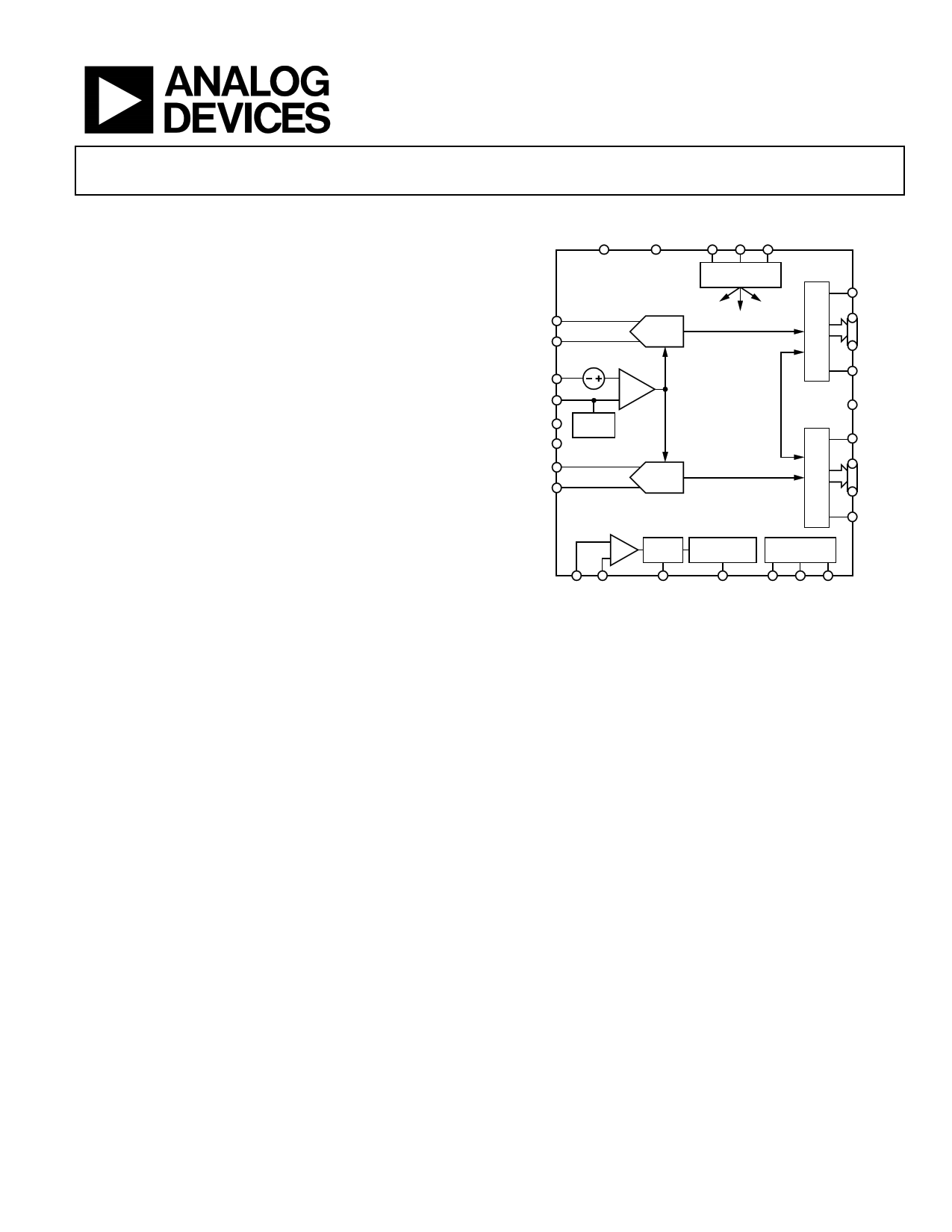
FUNCTIONAL BLOCK DIAGRAM
AVDD
GND
SDIO SCLK CSB
VIN+A
VIN–A
VREF
SENSE
VCM
RBIAS
VIN–B
VIN+B
REF
SELECT
SPI
ADC
PROGRAMMING DATA
AD9251
ADC
DIVIDE DUTY CYCLE
1 TO 8 STABILIZER
MODE
CONTROLS
ORA
D13A
D0A
DCOA
DRVDD
ORB
D13B
D0B
DCOB
CLK+ CLK–
SYNC
DCS
Figure 1.
PDWN DFS OEB
PRODUCT HIGHLIGHTS
1. The AD9251 operates from a single 1.8 V analog power
supply and features a separate digital output driver supply
to accommodate 1.8 V to 3.3 V logic families.
2. The patented sample-and-hold circuit maintains excellent
performance for input frequencies up to 200 MHz and is
designed for low cost, low power, and ease of use.
3. A standard serial port interface supports various product
features and functions, such as data output formatting,
internal clock divider, power-down, DCO/DATA timing
and offset adjustments, and voltage reference modes.
4. The AD9251 is packaged in a 64-lead RoHS compliant
LFCSP that is pin compatible with the AD9268 16-bit
ADC, the AD9258 14-bit ADC, the AD9231 12-bit ADC,
and the AD9204 10-bit ADC, enabling a simple migration
path between 10-bit and 16-bit converters sampling from
20 MSPS to 125 MSPS.
Rev. B
Document Feedback
Information furnished by Analog Devices is believed to be accurate and reliable. However, no
responsibilityisassumedbyAnalogDevices for itsuse,nor foranyinfringementsofpatentsor other
rights of third parties that may result from its use. Specifications subject to change without notice. No
license is granted by implication or otherwise under any patent or patent rights of Analog Devices.
Trademarksandregisteredtrademarksarethepropertyoftheirrespectiveowners.
One Technology Way, P.O. Box 9106, Norwood, MA 02062-9106, U.S.A.
Tel: 781.329.4700 ©2009–2016 Analog Devices, Inc. All rights reserved.
Technical Support
www.analog.com
1 page 
AD9251
Data Sheet
SPECIFICATIONS
DC SPECIFICATIONS
AVDD = 1.8 V; DRVDD = 1.8 V, maximum sample rate, 2 V p-p differential input, 1.0 V internal reference; AIN = −1.0 dBFS,
DCS disabled, unless otherwise noted.
Table 1.
Parameter
RESOLUTION
ACCURACY
No Missing Codes
Offset Error
Gain Error1
Differential Nonlinearity (DNL)2
Integral Nonlinearity (INL)2
MATCHING CHARACTERISTICS
Offset Error
Gain Error1
TEMPERATURE DRIFT
Offset Error
INTERNAL VOLTAGE REFERENCE
Output Voltage (1 V Mode)
Load Regulation Error at 1.0 mA
INPUT-REFERRED NOISE
VREF = 1.0 V
ANALOG INPUT
Input Span, VREF = 1.0 V
Input Capacitance3
Input Common-Mode Voltage
Input Common-Mode Range
REFERENCE INPUT RESISTANCE
POWER SUPPLIES
Supply Voltage
AVDD
DRVDD
Supply Current
IAVDD2
IDRVDD2 (1.8 V)
IDRVDD2 (3.3 V)
POWER CONSUMPTION
DC Input
Sine Wave Input2 (DRVDD = 1.8 V)
Sine Wave Input2 (DRVDD = 3.3 V)
Standby Power4
Power-Down Power
Temp
Full
AD9251-20/AD9251-40
Min Typ
Max
14
Full Guaranteed
Full ±0.1 ±0.70
Full −1.5
Full ±0.60
25°C ±0.3
Full ±1.75
25°C ±0.6
25°C ±0.0 ±0.65
25°C ±0.2
Full ±2
Full 0.981 0.993
Full 2
1.005
25°C 0.98
Full 2
Full 6
Full 0.9
Full 0.5
Full 7.5
1.3
AD9251-65
Min Typ Max
14
AD9251-80
Min Typ Max
14
Unit
Bits
Guaranteed
±0.1 ±0.50
−1.5
±0.75
±0.45
±1.75
±0.6
Guaranteed
±0.1 ±0.70
−1.5
±0.70
±0.45
±2.50
±1.0
% FSR
% FSR
LSB
LSB
LSB
LSB
±0.0 ±0.65
±0.2
±0.0 ±0.65 % FSR
±0.2 % FSR
±2 ±2 ppm/°C
0.981 0.993 1.005 0.981 0.993 1.005 V
2 2 mV
0.98 0.98 LSB rms
2 2 V p-p
6 6 pF
0.9 0.9 V
0.5 1.3 0.5 1.3 V
7.5 7.5 kΩ
Full 1.7 1.8
Full 1.7
1.9
3.6
1.7 1.8 1.9 1.7 1.8 1.9 V
1.7 3.6 1.7 3.6 V
Full
36.5/49.5 39.4/52.8
69.0 72.9
80.5 85.5 mA
Full 3.4/5.6
8.4 10.3 mA
Full 6.3/10.6
16.0 19.5 mA
Full 66/89
125 145 mW
Full
71.8/99 77.0/105.5
139.0 146.5
163.4 173 mW
Full 86.5/124
176.7
209 mW
Full 37
37 37 mW
Full 2.2
2.2 2.2 mW
1 Measured with 1.0 V external reference.
2 Measured with a 10 MHz input frequency at rated sample rate, full-scale sine wave, with approximately 5 pF loading on each output bit.
3 Input capacitance refers to the effective capacitance between one differential input pin and AGND.
4 Standby power is measured with a dc input and the CLK active.
Rev. B | Page 4 of 36
5 Page 
AD9251
ABSOLUTE MAXIMUM RATINGS
Table 6.
Parameter
AVDD to AGND
DRVDD to AGND
VIN+A, VIN+B, VIN−A, VIN−B to AGND
CLK+, CLK− to AGND
SYNC to AGND
VREF to AGND
SENSE to AGND
VCM to AGND
RBIAS to AGND
CSB to AGND
SCLK/DFS to AGND
SDIO/DCS to AGND
OEB to AGND
PDWN to AGND
D0A/D0B through D13A/D13B to AGND
DCOA/DCOB to AGND
Operating Temperature Range (Ambient)
Maximum Junction Temperature
Under Bias
Storage Temperature Range (Ambient)
Rating
−0.3 V to +2.0 V
−0.3 V to +3.9 V
−0.3 V to AVDD + 0.2 V
−0.3 V to AVDD + 0.2 V
−0.3 V to DRVDD + 0.3 V
−0.3 V to AVDD + 0.2 V
−0.3 V to AVDD + 0.2 V
−0.3 V to AVDD + 0.2 V
−0.3 V to AVDD + 0.2 V
−0.3 V to DRVDD + 0.3 V
−0.3 V to DRVDD + 0.3 V
−0.3 V to DRVDD + 0.3 V
−0.3 V to DRVDD + 0.3 V
−0.3 V to DRVDD + 0.3 V
−0.3 V to DRVDD + 0.3 V
−0.3 V to DRVDD + 0.3 V
−40°C to +85°C
150°C
−65°C to +150°C
Stresses at or above those listed under Absolute Maximum
Ratings may cause permanent damage to the product. This is a
stress rating only; functional operation of the product at these
or any other conditions above those indicated in the operational
section of this specification is not implied. Operation beyond
the maximum operating conditions for extended periods may
affect product reliability.
Data Sheet
THERMAL CHARACTERISTICS
The exposed paddle is the only ground connection for the chip.
The exposed paddle must be soldered to the AGND plane of the
user’s circuit board. Soldering the exposed paddle to the user’s
board also increases the reliability of the solder joints and
maximizes the thermal capability of the package.
Typical θJA is specified for a 4-layer PCB with a solid ground
plane. As shown in Table 7, airflow improves heat dissipation,
which reduces θJA. In addition, metal in direct contact with the
package leads from metal traces, through holes, ground, and
power planes, reduces the θJA.
Table 7. Thermal Resistance
Package Type
Airflow
Velocity
(m/sec)
θJA1, 2
64-Lead LFCSP 0
23
(CP-64-4)
1.0
20
2.5 18
θJC1, 3
2.0
θJB1, 4
12
1 Per JEDEC 51-7, plus JEDEC 25-5 2S2P test board.
2 Per JEDEC JESD51-2 (still air) or JEDEC JESD51-6 (moving air).
3 Per MIL-Std 883, Method 1012.1.
4 Per JEDEC JESD51-8 (still air).
Unit
°C/W
°C/W
°C/W
ESD CAUTION
Rev. A | Page 10 of 36
11 Page | ||
| Páginas | Total 30 Páginas | |
| PDF Descargar | [ Datasheet AD9251.PDF ] | |
Hoja de datos destacado
| Número de pieza | Descripción | Fabricantes |
| AD9250 | Dual Analog-to-Digital Converter | Analog Devices |
| AD9251 | 1.8 V Dual Analog-to-Digital Converter | Analog Devices |
| AD9252 | 1.8 V ADC | Analog Devices |
| AD9253 | 80 MSPS/105 MSPS/125 MSPS | Analog Devices |
| Número de pieza | Descripción | Fabricantes |
| SLA6805M | High Voltage 3 phase Motor Driver IC. |
Sanken |
| SDC1742 | 12- and 14-Bit Hybrid Synchro / Resolver-to-Digital Converters. |
Analog Devices |
|
DataSheet.es es una pagina web que funciona como un repositorio de manuales o hoja de datos de muchos de los productos más populares, |
| DataSheet.es | 2020 | Privacy Policy | Contacto | Buscar |