|
|
|
PDF LM5041B Data sheet ( Hoja de datos )
| Número de pieza | LM5041B | |
| Descripción | Cascaded PWM Controller | |
| Fabricantes | National Semiconductor | |
| Logotipo | ||
Hay una vista previa y un enlace de descarga de LM5041B (archivo pdf) en la parte inferior de esta página. Total 16 Páginas | ||
|
No Preview Available !
www.DataSheet4U.com
LM5041B
May 1, 2009
Cascaded PWM Controller
General Description
The LM5041B PWM controller contains all of the features
necessary to implement either current-fed or voltage-fed
push-pull or bridge power converters. These “Cascaded”
topologies are well suited for multiple output and higher power
applications. The LM5041B includes these four control out-
puts: the buck stage controls (HD and LD) and the push-pull
control outputs (PUSH and PULL). Push-pull outputs are driv-
en at 50% nominal duty cycle at one half of the switching
frequency of the buck stage and can be configured for either
a guaranteed overlap time (for current-fed applications) or a
guaranteed non-overlap time (for voltage-fed applications).
Push-pull stage MOSFETs can be driven directly from the in-
ternal gate drivers while the buck stage requires an external
driver such as the LM5102. The LM5041B includes a high-
voltage start-up regulator that operates over a wide input
range of 15V to 100V. The PWM controller is designed for
high-speed capability including an oscillator frequency range
up to 1 MHz and total propagation delays of less than 100 ns.
Additional features include line Under-Voltage Lock-Out
(UVLO), Soft-Start, an error amplifier, precision voltage ref-
erence, and thermal shutdown.
The differences between LM5041, LM5041A and LM5041B
are as follows: In the LM5041A and the LM5041B version, the
hiccup mode over-current protection is not employed and the
VCC bias regulator is not disabled by a low state at the SS
pin. In the LM5041B version, both the high and low side buck
stage gate drivers are forced to a low state when the controller
is disabled. In the LM5041 and the LM5041B version, the
buck stage controller is disabled by either a low state at the
UVLO pin or a low state at the SS pin. Also in the LM5041B
version, the REF pin 5V regulator is not disabled by a UVLO
pin low state.
Features
■ Internal Start-up Bias Regulator
■ Programmable Line Under-Voltage Lockout (UVLO) with
Adjustable Hysteresis
■ Current Mode Control
■ Internal Error Amplifier with Reference
■ Cycle-by-cycle Over-Current Protection
■ Leading Edge Blanking
■ Programmable Push-Pull Overlap or Dead Time
■ Internal 1.5A Push-Pull Gate Drivers
■ Programmable Soft-Start
■ Programmable Oscillator with Sync Capability
■ Precision Reference
■ Thermal Shutdown
Applications
■ Telecommunication Power Converters
■ Industrial Power Converters
■ Multi-Output Power Converters
Packages
■ TSSOP-16
■ LLP-16 (5x5 mm) Thermally Enhanced
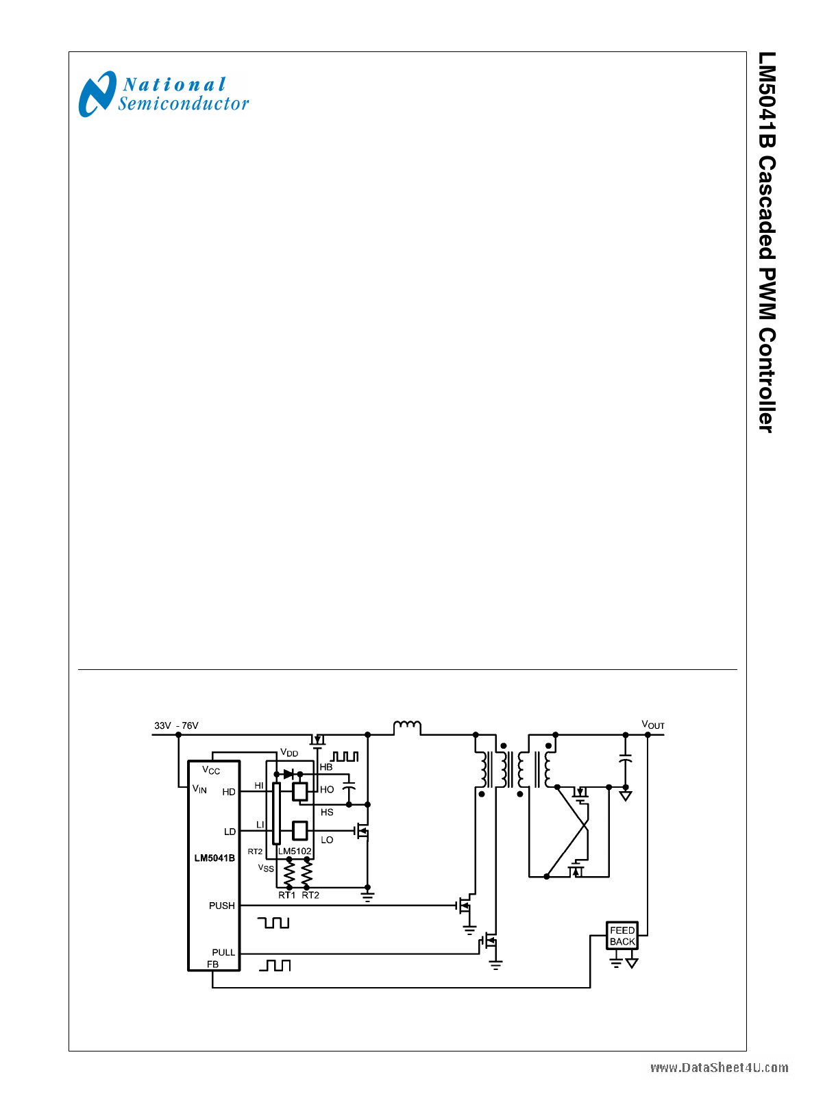
Typical Application Circuit
Simplified Cascaded Push-Pull Power Converter
© 2009 National Semiconductor Corporation 300864
30086401
www.national.com
1 page 
Symbol
Parameter
Owswcwil.lDaatotarSheet4U.com
Conditions
Frequency1
RT = 26.7 kΩ
Frequency2
Sync threshold
PWM Comparator
Delay to Output
RT = 7.87 kΩ
COMP = 2V, CS stepped 0 to 0.4V
Time to onset of OUT transition low
Max Duty Cycle
TS = Oscillator Period
Min Duty Cycle
COMP to PWM Comparator Gain
COMP Open Circuit Voltage
COMP Short Circuit Current
Slope Compensation
Slope Comp Amplitude
UVLO Shutdown
Under-Voltage Shutdown
Under-voltage Shutdown
Hysteresis Current Source
Buck Stage Outputs
Output High level
Output High Saturation
Output Low Saturation
Rise Time
Fall Time
Push-Pull Outputs
Overlap Time
Dead Time
Output High Saturation
Output Low Saturation
Rise Time
Fall Time
Thermal Shutdown
TSD Thermal Shutdown Temp.
Thermal Shutdown Hysteresis
Thermal Resistance
Thermal Resistance
θJA Junction to Ambient
COMP = 0V
FB = 0V
FB = 0V, COMP = 0V
Delta increase at PWM Comparator
to CS
IOUT = 10 mA, REF = VOUT
IOUT = −10 mA
CL = 100 pF
CL = 100 pF
RSET = 20 kΩ Connected to GND,
50% to 50% Transitions
RSET = 20kΩ Connected to REF,
50% to 50% Transitions
IOUT = 50 mA
VCC - VOUT
IOUT = 100 mA
CL = 1 nF
CL = 1 nF
TSSOP Package
LLP Package
Min
180
175
515
-
-
-
-
-
4.1
0.6
-
2.44
16
-
-
-
-
-
60
65
-
-
-
-
-
-
-
-
Typ
200
600
3
25
(Ts-240ns)
/ Ts
-
0.32
4.8
1
110
2.5
20
5 (VREF)
0.5
0.5
10
10
90
95
0.25
0.5
20
20
165
25
125
32
Max
220
225
685
3.5
-
-
0
-
5.5
1.4
-
2.56
24
-
1
1
-
-
120
125
0.5
1
-
-
-
-
-
Units
kHz
kHz
V
ns
%
%
V
mA
mV
V
µA
V
V
V
ns
ns
ns
ns
V
V
ns
ns
°C
°C
°C/W
°C/W
Note 1: Absolute Maximum Ratings indicate limits beyond which damage to the device may occur. Operating Ratings indicate conditions for which the device is
intended to be functional, but does not guarantee specific performance limits. For guaranteed specifications and conditions, see the Electrical Characteristics.
Note 2: The human body model is a 100 pF capacitor discharged through a 1.5 kΩ resistor into each pin. Test Method is per JESD-22-A114.
Note 3: For detailed information on soldering plastic TSSOP and LLP packages, please refer to Application Note AN-1520: A Guide to Board Layout for Best
Thermal Resistance for Exposed Packages , Application Note AN-1187: Leadless Leadframe Package (LLP) , or go to www.national.com/packaging for more
information.
Note 4: Device thermal limitations may limit usable range.
5 www.national.com
5 Page 
wwSwl.oDaptaeShCeeto4Um.copmensation
The PWM comparator compares the current sense signal to
the voltage at the COMP pin. The output stage of the internal
error amplifier generally drives the COMP pin. At duty cycles
greater than 50%, current mode control circuits are subject to
sub-harmonic oscillation. By adding an additional fixed ramp
signal (slope compensation) to the current sense ramp, os-
cillations can be avoided. The LM5041B integrates this slope
compensation by buffering the internal oscillator ramp and
summing a current ramp generated by the oscillator internally
with the current sense signal. Additional slope compensation
may be provided by increasing the source impedance of the
current sense signal.
Soft-Start and Shutdown
The soft-start feature allows the power converter to gradually
reach the initial steady state operating point, thereby reducing
start-up stresses and surges. At power on, a 10 µA current is
sourced out of the soft-start pin (SS) to charge an external
capacitor. The capacitor voltage will ramp up slowly and will
limit the maximum duty cycle of the buck stage. In the event
of a fault as indicated by VCC Under-voltage, line Under-volt-
age the output drivers are disabled and the soft-start capacitor
is discharged to 0.7V. When the fault condition is no longer
present, a soft-start sequence will begin again and buck stage
duty cycle will gradually increase as the soft-start capacitor is
charged.
The SS pin also serves as an enable input of HD and LD. Both
HD and LD will be forced to a low state if the SS pin is below
the shutdown threshold of 0.45V.
Thermal Protection
Internal Thermal Shutdown circuitry is provided to protect the
integrated circuit in the event that the maximum junction tem-
perature is exceeded. When activated, typically at 165 de-
grees Celsius, the controller is forced into a low-power
standby state, disabling the output drivers and the bias regu-
lator. This feature is provided to prevent catastrophic failures
from accidental device overheating.
Differences Between LM5041,
LM5041A and LM5041B
There are five differences between LM5041, LM5041A and
LM5041B. In the LM5041A and the LM5041B versions, the
hiccup mode over-current protection is not employed and the
VCC bias regulator is not disabled by SS pin shutdown state.
In the LM5041B version, both HD and LD will be low state
when the PWM controller disabled. In the LM5041 and the
LM5041B version, PWM controller is disabled by either a UV-
LO pin low state or SS pin shutdown state. Also in the
LM5041B version, the REF pin output is not disabled by a
UVLO pin low state. However, if VCC does not receive power
from an external source, the UVLO pin low state will disable
the internal VCC regulator and a VCC under-voltage condition
will eventually disable REF as the VCC voltage falls.
Differences Between LM5041, LM5041A and LM5041B
ITEM
Hiccup mode over-current protection
VCC disabled by SS shutdown
REF disabled by UVLO pin low state
BUCK controller disabled by SS shutdown
BUCK driver states when the controller disabled
LM5041
Available
Yes
Yes
Yes
HD : LOW
LD :HIGH
LM5041A
N/A
No
Yes
No
HD : LOW
LD : HIGH
LM5041B
N/A
No
No
Yes
HD : LOW
LD : LOW
Logic Table
MODE
CONTROLS
UVLO
SS
Normal
Operation
HIGH
-
UVLO
Shutdown
LOW
-
SS
Shutdown
HIGH
LOW
DEVICE
LM5041
LM5041A
LM5041B
LM5041
LM5041A
LM5041B
LM5041
LM5041A
LM5041B
VCC
9V
GND
GND
9V
REF
5V
GND
GND
5V
PIN STATES
HD
LD
PWM
PWM
PUSH&PULL
50% Duty Cycle
LOW
LOW
HIGH
LOW
HIGH
LOW
LOW
LOW
50% Duty Cycle
11 www.national.com
11 Page | ||
| Páginas | Total 16 Páginas | |
| PDF Descargar | [ Datasheet LM5041B.PDF ] | |
Hoja de datos destacado
| Número de pieza | Descripción | Fabricantes |
| LM5041 | Cascaded PWM Controller | National Semiconductor |
| LM5041 | LM5041 Cascaded PWM Controller (Rev. D) | Texas Instruments |
| LM5041A | LM5041A Cascaded PWM Controller (Rev. B) | Texas Instruments |
| LM5041A | Cascaded PWM Controller | National Semiconductor |
| Número de pieza | Descripción | Fabricantes |
| SLA6805M | High Voltage 3 phase Motor Driver IC. |
Sanken |
| SDC1742 | 12- and 14-Bit Hybrid Synchro / Resolver-to-Digital Converters. |
Analog Devices |
|
DataSheet.es es una pagina web que funciona como un repositorio de manuales o hoja de datos de muchos de los productos más populares, |
| DataSheet.es | 2020 | Privacy Policy | Contacto | Buscar |