|
|
|
PDF PV1010UDF8B Data sheet ( Hoja de datos )
| Número de pieza | PV1010UDF8B | |
| Descripción | ESD/EMI Filter | |
| Fabricantes | KEC | |
| Logotipo | ||
Hay una vista previa y un enlace de descarga de PV1010UDF8B (archivo pdf) en la parte inferior de esta página. Total 2 Páginas | ||
|
No Preview Available !
www.DataSheet4U.com
SEMICONDUCTOR
TECHNICAL DATA
PV1010UDF8B
ESD/EMI Filter
APPLICATION
I/O ESD protection for mobile handsets, notebook, PDAs, etc.
EMI filtering for data ports in cell phones, PDAs, notebook computers
EMI filtering for LCD, camera and chip-to-chip data lines
FEATURES
EMI/RFI filtering
ESD Protection to IEC 61000-4-2 Level 4
Low insertion loss
Good attenuation of high frequency signals
Low clamping voltage
Low operating and leakage current
Four elements in one package
DESCRIPTION
PV1010UDF8B is an EMI filter array with electrostatic discharge (ESD) protection,
which integrates four pi filters (C-R-C). These parts include ESD protection diodes on
every pin, providing a very high level of protection for sensitive electronic components
that may be subjected to electrostatic discharge.
The PV1010UDF8B provides the recommended line termination while implementing a
low pass filter to limit EMI levels and providing ESD protection which exceeds IEC
61000-4-2 level 4 standard. The UDFN package is a very effective PCB space
occupation and a very thin package (0.4mm Pitch, 0.5mm height)
MAXIMUM RATING (Ta=25 )
CHARACTERISTIC
DC Power Per Resistor
Power Dissipation
Junction Temperature
Storage Temperature
* Total Package Power Dissipation
SYMBOL
PR
*PD
Tj
Tstg
RATING
100
400
150
-55 150
UNIT
mW
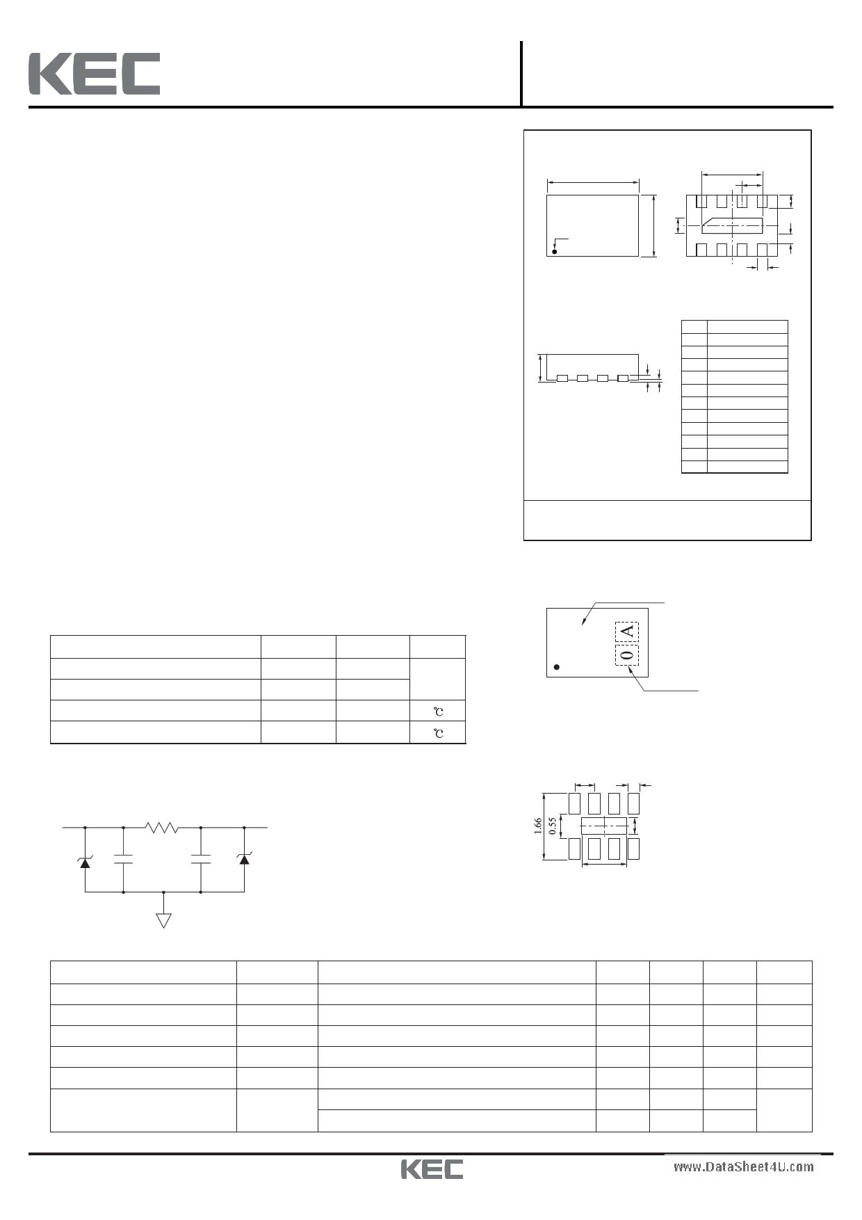
EQUIVALENT CIRCUIT
FILTERn*
100Ω
FILTERn*
10pF
10pF
A
Pin 1
TOP VIEW
C
E
14
GND PAD
8 D5
BOTTOM VIEW
K
L
SIDE VIEW
1,8 : Filter channel 1
2,7 : Filter channel 2
3,6 : Filter channel 3
4,5 : Filter channel 4
DIM
A
B
C
D
E
F
G
H
J
K
L
MILLIMETERS
1.70 +_ 0.10
1.35 +_ 0.10
1.20 +_ 0.10
0.20 +_ 0.05
0.40
0.40 +_ 0.10
0.25 +_ 0.10
0.20 Min
0.50 +_ 0.05
0.127
0.02+0.03/-0.02
UDFN-8B
MARKING
Type Name
V2
Lot No.
RECOMMENEDED FOOTPRINT
(dimensions in mm)
0.40
0.30
GND 0.25
0.70
GND
ELECTRICAL CHARACTERISTICS (Ta=25 )
CHARACTERISTIC
Reverse Stand-Off Voltage
Reverse Breakdown Voltage
Reverse Leakage Current
Cutoff Frequency
Channel Resistance
Line Capacitance
SYMBOL
VRWM
VBR
IR
fc-3dB
RLINE
CLINE
TEST CONDITION
-
It=1mA
VRWM=3.3V
VLine=0V, ZSOURCE=50 , ZLOAD=50
Between Input and Output
VLine=0V DC, 1MHz, Between I/O Pins and GND
VLine=2.5V, 1MHz, Between I/O Pins and GND
MIN.
-
6
-
-
80
24
16
TYP.
-
-
-
150
100
30
20
MAX.
5
-
1.0
-
120
36
24
UNIT
V
V
A
MHz
pF
2009. 6. 3
Revision No : 0
1/2
1 page | ||
| Páginas | Total 2 Páginas | |
| PDF Descargar | [ Datasheet PV1010UDF8B.PDF ] | |
Hoja de datos destacado
| Número de pieza | Descripción | Fabricantes |
| PV1010UDF8B | ESD/EMI Filter | KEC |
| Número de pieza | Descripción | Fabricantes |
| SLA6805M | High Voltage 3 phase Motor Driver IC. |
Sanken |
| SDC1742 | 12- and 14-Bit Hybrid Synchro / Resolver-to-Digital Converters. |
Analog Devices |
|
DataSheet.es es una pagina web que funciona como un repositorio de manuales o hoja de datos de muchos de los productos más populares, |
| DataSheet.es | 2020 | Privacy Policy | Contacto | Buscar |