|
|
|
PDF ADCLK948 Data sheet ( Hoja de datos )
| Número de pieza | ADCLK948 | |
| Descripción | SiGe Clock Fanout Buffer | |
| Fabricantes | Analog Devices | |
| Logotipo | ||
Hay una vista previa y un enlace de descarga de ADCLK948 (archivo pdf) en la parte inferior de esta página. Total 12 Páginas | ||
|
No Preview Available !
Two Selectable Inputs, 8 LVPECL Outputs,
SiGe Clock Fanout Buffer
ADCLK948
FEATURES
2 selectable differential inputs
4.8 GHz operating frequency
75 fs rms broadband random jitter
On-chip input terminations
3.3 V power supply
APPLICATIONS
Low jitter clock distribution
Clock and data signal restoration
Level translation
Wireless communications
Wired communications
Medical and industrial imaging
ATE and high performance instrumentation
GENERAL DESCRIPTION
The ADCLK948 is an ultrafast clock fanout buffer fabricated
on the Analog Devices, Inc., proprietary XFCB3 silicon german-
ium (SiGe) bipolar process. This device is designed for high
speed applications requiring low jitter.
The device has two selectable differential inputs via the IN_SEL
control pin. Both inputs are equipped with center tapped,
differential, 100 Ω on-chip termination resistors. The inputs
accept dc-coupled LVPECL, CML, 3.3 V CMOS (single-ended),
and ac-coupled 1.8 V CMOS, LVDS, and LVPECL inputs. A
VREFx pin is available for biasing ac-coupled inputs.
The ADCLK948 features eight full-swing emitter coupled logic
www.Da(EtaCSLh)eoetu4tUp.uctodmrivers. For LVPECL (positive ECL) operation,
bias VCC to the positive supply and VEE to ground. For ECL
operation, bias VCC to ground and VEE to the negative supply.
The output stages are designed to directly drive 800 mV each
side into 50 Ω terminated to VCC − 2 V for a total differential
output swing of 1.6 V.
The ADCLK948 is available in a 32-lead LFCSP and specified
for operation over the standard industrial temperature range of
−40°C to +85°C.
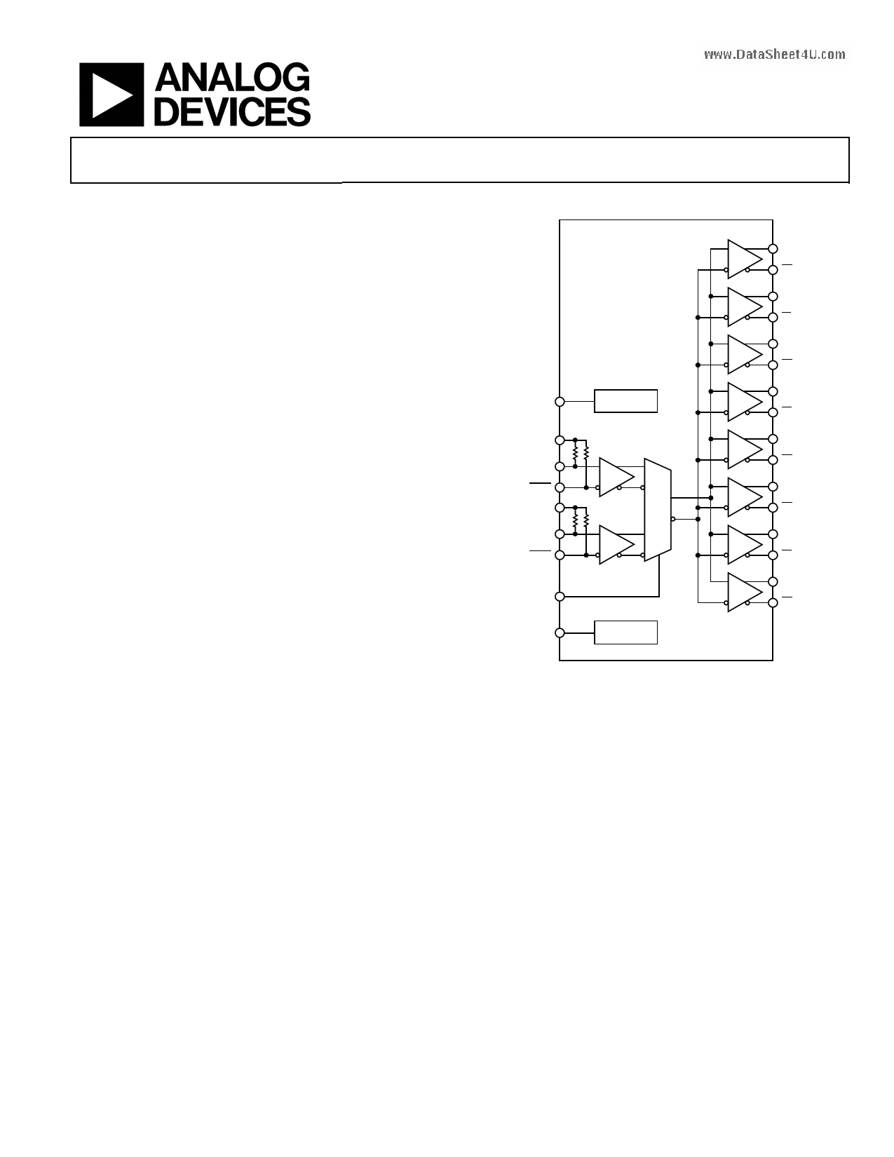
FUNCTIONAL BLOCK DIAGRAM
ADCLK948
LVPECL
Q0
Q0
Q1
Q1
Q2
Q2
VREF0
REFERENCE
Q3
Q3
VT0
CLK0
CLK0
VT1
CLK1
CLK1
Q4
Q4
Q5
Q5
Q6
Q6
IN_SEL
Q7
Q7
VREF1
REFERENCE
Figure 1.
Rev. 0
Information furnished by Analog Devices is believed to be accurate and reliable. However, no
responsibility is assumed by Analog Devices for its use, nor for any infringements of patents or other
rights of third parties that may result from its use. Specifications subject to change without notice. No
license is granted by implication or otherwise under any patent or patent rights of Analog Devices.
Trademarksandregisteredtrademarksarethepropertyoftheirrespectiveowners.
One Technology Way, P.O. Box 9106, Norwood, MA 02062-9106, U.S.A.
Tel: 781.329.4700
www.analog.com
Fax: 781.461.3113
©2009 Analog Devices, Inc. All rights reserved.
1 page 
ABSOLUTE MAXIMUM RATINGS
Table 5.
Parameter
Supply Voltage
VCC − VEE
Input Voltage
CLK0, CLK1, CLK0, CLK1, IN_SEL
CLK0, CLK1, CLK0, CLK1 to VTx Pin (CML,
LVPECL Termination)
CLK0, CLK1 to CLK0, CLK1
Input Termination, VTx to CLK0, CLK1, CLK0,
and CLK1
Maximum Voltage on Output Pins
Maximum Output Current
Voltage Reference (VREFx)
Operating Temperature Range
Ambient
Junction
Storage Temperature Range
Rating
6V
VEE − 0.5 V to
VCC + 0.5 V
±40 mA
±1.8 V
±2 V
VCC + 0.5 V
35 mA
VCC to VEE
−40°C to +85°C
150°C
−65°C to +150°C
Stresses above those listed under Absolute Maximum Ratings
may cause permanent damage to the device. This is a stress
rating only; functional operation of the device at these or any
other conditions above those indicated in the operational
section of this specification is not implied. Exposure to absolute
maximum rating conditions for extended periods may affect
device reliability.
ADCLK948
DETERMINING JUNCTION TEMPERATURE
To determine the junction temperature on the application
printed circuit board (PCB), use the following equation:
TJ = TCASE + (ΨJT × PD)
where:
TJ is the junction temperature (°C).
TCASE is the case temperature (°C) measured by the customer at
the top center of the package.
ΨJT is from Table 6.
PD is the power dissipation.
Values of θJA are provided for package comparison and PCB
design considerations. θJA can be used for a first-order approxi-
mation of TJ by the equation
TJ = TA + (θJA × PD)
where TA is the ambient temperature (°C).
Values of θJB are provided in Table 6 for package comparison
and PCB design considerations.
ESD CAUTION
THERMAL PERFORMANCE
Table 6.
www.DataSheet4U.com
Parameter
Junction-to-Ambient Thermal Resistance
Still Air
0 m/sec Air Flow
Moving Air
1 m/sec Air Flow
2.5 m/sec Air Flow
Junction-to-Board Thermal Resistance
Moving Air
1 m/sec Air Flow
Junction-to-Case Thermal Resistance
Moving Air
Die-to-Heatsink
Junction-to-Top-of-Package Characterization Parameter
Still Air
0 m/sec Air Flow
Symbol
θJA
Description
Per JEDEC JESD51-2
θJMA Per JEDEC JESD51-6
θJB
Per JEDEC JESD51-8
θJC
Per MIL-STD 883, Method 1012.1
ΨJT
Per JEDEC JESD51-2
Value1 Unit
49.8 °C/W
43.5 °C/W
39.0 °C/W
30.7 °C/W
8.8 °C/W
0.7 °C/W
1 Results are from simulations. The PCB is a JEDEC multilayer type. Thermal performance for actual applications requires careful inspection of the conditions in the
application to determine if they are similar to those assumed in these calculations.
Rev. 0 | Page 5 of 12
5 Page 
INPUT TERMINATION OPTIONS
VCC
VREFx
VTx
50Ω
CLKx
CLKx
50Ω
ADCLK948
CONNECT VTx TO VCC.
Figure 19. DC-Coupled CML Input Termination
VCC
0.01µF
(OPTIONAL)
50Ω
VREFx
VTx
50Ω
CLKx
CLKx
50Ω
ADCLK948
Figure 20. DC-Coupled LVPECL Input Termination
www.DataSheet4U.com
ADCLK948
VREFx
VTx
50Ω
CLKx
CLKx
50Ω
ADCLK948
CONNECT VTx TO VREFx.
Figure 21. AC-Coupled Input Termination, Such as LVDS and LEVPECL
VREFx
VTx
50Ω
CLKx
CLKx
50Ω
ADCLK948
CONNECT VTx, VREFx, AND CLKx. PLACE A
BYPASS CAPACITOR FROM VTx TO GROUND.
ALTERNATIVELY, VTx, VREFx, AND CLKx CAN BE
CONNECTED, GIVING A CLEANER LAYOUT AND
A 180º PHASE SHIFT.
Figure 22. AC-Coupled Single-Ended Input Termination
VREFx
VTx
50Ω
CLKx
CLKx
50Ω
ADCLK948
Figure 23. DC-Coupled 3.3 V CMOS Input Termination
Rev. 0 | Page 11 of 12
11 Page | ||
| Páginas | Total 12 Páginas | |
| PDF Descargar | [ Datasheet ADCLK948.PDF ] | |
Hoja de datos destacado
| Número de pieza | Descripción | Fabricantes |
| ADCLK944 | SIGE CLOCK FANOUT BUFFER | Analog Devices |
| ADCLK946 | SiGe Clock Fanout Buffer | Analog Devices |
| ADCLK948 | SiGe Clock Fanout Buffer | Analog Devices |
| Número de pieza | Descripción | Fabricantes |
| SLA6805M | High Voltage 3 phase Motor Driver IC. |
Sanken |
| SDC1742 | 12- and 14-Bit Hybrid Synchro / Resolver-to-Digital Converters. |
Analog Devices |
|
DataSheet.es es una pagina web que funciona como un repositorio de manuales o hoja de datos de muchos de los productos más populares, |
| DataSheet.es | 2020 | Privacy Policy | Contacto | Buscar |