|
|
|
PDF AGR21090E Data sheet ( Hoja de datos )
| Número de pieza | AGR21090E | |
| Descripción | Transistor | |
| Fabricantes | TriQuint Semiconductor | |
| Logotipo | ||
Hay una vista previa y un enlace de descarga de AGR21090E (archivo pdf) en la parte inferior de esta página. Total 9 Páginas | ||
|
No Preview Available !
AGR21090E
90 W, 2.110 GHz—2.170 GHz, N-Channel E-Mode, Lateral MOSFET
Introduction
The AGR21090E is a high-voltage, gold-metalized,
laterally diffused, metal oxide semiconductor
(LDMOS) RF power transistor suitable for wideband
code-division multiple access (W-CDMA), and single
and multicarrier class AB wireless base station power
amplifier applications.
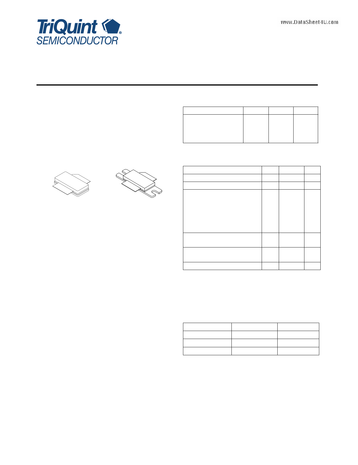
AGR21090EU (unflanged) AGR21090EF (flanged)
Figure 1. Available Packages
Features
Typical performance for 2 carrier 3GPP
W-CDMA systems. F1 = 2135 MHz and
F2 = 2145 MHz with 3.84 MHz channel BW, adja-
cent channel BW = 3.84 MHz at F1 – 5 MHz and
www.DataShFe2et4+U5.coMmHz. Third-order distortion is measured
over 3.84 MHz BW at F1 – 10 MHz and
F2 + 10 MHz. Typical P/A ratio of 8.5 dB at 0.01%
(probability) CCDF:
— Output power: 19 W.
— Power gain: 14.5 dB.
— Efficiency: 26%.
— IM3: –33 dBc.
— ACPR: –36 dBc.
— Return loss: –12 dB.
High-reliability, gold-metalization process.
Low hot carrier injection (HCI) induced bias drift
over 20 years.
Internally matched.
High gain, efficiency, and linearity.
Integrated ESD protection.
Device can withstand a 10:1 voltage standing wave
ratio (VSWR) at 28 Vdc, 2140 MHz, 90 W continu-
ous wave (CW) output power.
Large signal impedance parameters available.
Table 1. Thermal Characteristics
Parameter
Thermal Resistance,
Junction to Case:
AGR21090EU
AGR21090EF
Sym
Rı JC
Rı JC
Value
0.7
0.7
Unit
°C/W
°C/W
Table 2. Absolute Maximum Ratings*
Parameter
Sym Value Unit
Drain-source Voltage
VDSS 65 Vdc
Gate-source Voltage
VGS –0.5, 15 Vdc
Total Dissipation at TC = 25 °C:
AGR21090EU
PD 250 W
AGR21090EF
PD 250 W
Derate Above 25 ˇC:
AGR21090EU
— 1.4 W/°C
AGR21090EF
— 1.4 W/°C
CW RF Input Power
— 30 W
(VDS = 31 V)
Operating Junction Tempera- TJ 200 °C
ture
Storage Temperature Range TSTG –65, 150 °C
* Stresses in excess of the absolute maximum ratings can cause
permanent damage to the device. These are absolute stress rat-
ings only. Functional operation of the device is not implied at
these or any other conditions in excess of those given in the
operational sections of the data sheet. Exposure to absolute
maximum ratings for extended periods can adversely affect
device reliability.
Table 3. ESD Rating*
AGR21090E
HBM
MM
CDM
Minimum (V)
500
50
1500
Class
1B
A
4
* Although electrostatic discharge (ESD) protection circuitry has
been designed into this device, proper precautions must be
tdaukreinngtoalal hvoainddelinxpgo, sausrseemtobElyS, Danadntdesetleocpterircaatlioonvse.rPsAtEgreeAsrKes (DEeOvSic)es
employs a human-body model (HBM), a machine model (MM),
and a charged-device model (CDM) qualification requirement in
order to determine ESD-susceptibility limits and protection
design evaluation. ESD voltage thresholds are dependent on the
circuit parameters used in each of the models, as defined by
JEDEC's JESD22-A114B (HBM), JESD22-A115A (MM), and
JESD22-C101A (CDM) standards.
Caution: MOS devices are susceptible to damage from elec-
trostatic charge. Reasonable precautions in han-
dling and packaging MOS devices should be
observed.
1 page 
AGR21090E
90 W, 2.110 GHz—2.170 GHz, N-Channel E-Mode, Lateral MOSFET
Typical Performance Characteristics (continued)
16.50
16.00
15.50
15.00
14.50
14.00
13.50
13.00
12.50
12.00
11.50
1.00
IDQ = 500 mA
Test Conditions:
VDD 28 Vdc, f1 = 2135 MHz, f2 = 2145 MHz.
Two-tone measurement, 10 MHz tone spacing.
IDQ = 1100 mA
IDQ = 950 mA
IDQ = 650 mA
10.00
POUT (W) PEPZ
IDQ = 800 mA
Figure 4. Two-Tone Power Gain vs. Output Power and IDQ
100.00
-20.00
-25.00
-30.00
IDQ = 500 mA
IDQ = 650 mA
-35.00
www.DataSheet4U.com
-40.00
-45.00
-50.00
-55.00
-60.00
-65.00
-70.00
1.00
IDQ = 800 mA
10.00
IDQ = 1100 mA
IDQ = 950 mA
100.00
POUT (W) PEPZ
Test Conditions:
VDD 28 Vdc, f1 = 2135 MHz, f2 = 2145 MHz.
Two-tone measurement, 10 MHz tone spacing.
Figure 5. IMD3 vs. Output Power and IDQ
1000.00
5 Page | ||
| Páginas | Total 9 Páginas | |
| PDF Descargar | [ Datasheet AGR21090E.PDF ] | |
Hoja de datos destacado
| Número de pieza | Descripción | Fabricantes |
| AGR21090E | Transistor | TriQuint Semiconductor |
| Número de pieza | Descripción | Fabricantes |
| SLA6805M | High Voltage 3 phase Motor Driver IC. |
Sanken |
| SDC1742 | 12- and 14-Bit Hybrid Synchro / Resolver-to-Digital Converters. |
Analog Devices |
|
DataSheet.es es una pagina web que funciona como un repositorio de manuales o hoja de datos de muchos de los productos más populares, |
| DataSheet.es | 2020 | Privacy Policy | Contacto | Buscar |