|
|
|
PDF MC33902 Data sheet ( Hoja de datos )
| Número de pieza | MC33902 | |
| Descripción | High Speed CAN Interface | |
| Fabricantes | Motorola Semiconductors | |
| Logotipo | ||
Hay una vista previa y un enlace de descarga de MC33902 (archivo pdf) en la parte inferior de esta página. Total 30 Páginas | ||
|
No Preview Available !
Freescale Semiconductor
Advance Information
Document Number: MC33902
Rev. 3.0, 8/2009
High Speed CAN Interface with
Embedded 5.0 V Supply
33902
The MC33902 is a high speed CAN physical interface. The device
includes an internal 5.0 V supply for the CAN bus transceiver, and
requires only a connection to a battery line.
The MC33902 provides 4 operation modes, including low power
modes with remote and local wake-up.
The device has very low sleep and standby current consumption.
Features
• High speed CAN interface for baud rates of 40 kb/s to 1.0 Mb/s
• Compatible to ISO11898 standard
• Single supply from battery. No need for a 5.0 V supply for CAN
interface
• I/O compatible from 2.75 V to 5.5 V via a dedicated input terminal
(3.3 V or 5.0 V logic compatible)
• Low Power mode with remote CAN wake-up and local wake-up
recognition and reporting
• CAN bus failure diagnostics and TXD/RXD pin monitoring, cold
start detection, wake-up sources reported through the ERR pin
• Enhanced diagnostics for bus, TXD, RXD and supply pins
available through Pseudo SPI via existing terminals EN, STBY
and ERR.
• Split terminal for bus recessive level stabilization
• INH output to control external voltage regulator
• Pb-free packaging designated by suffix code EF
HIGH SPEED CAN PHYSICAL INTERFACE
EF SUFFIX (PB-FREE)
98ASB42565B
14-PIN SOICN
ORDERING INFORMATION
Device
MCZ33902EF/R2
Temperature
Range (TA)
-40°C to 125°C
Package
14 SOIC
www.DataSheet4U.com
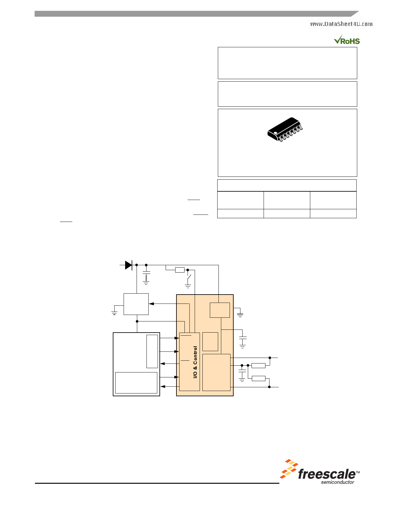
VBAT
Voltage
Regulator
INH
VDD
MCU
I/O
CAN
Controller
Tx
Rx
WAKE
INH
VIO
33902
VSUP
5V Reg
GND
VDD
STBY
EN
ERR
TXD
RXD
Bus
Diag.
CANH
SPLIT
Bus Driver
& Receiver
CANL
30
CAN bus
30
Figure 1. MC33902 Simplified Application Diagram
* This document contains certain information on a new product.
Specifications and information herein are subject to change without notice.
© Freescale Semiconductor, Inc., 2007-2009. All rights reserved.
1 page 
ELECTRICAL CHARACTERISTICS
STATIC ELECTRICAL CHARACTERISTICS
STATIC ELECTRICAL CHARACTERISTICS
Table 3. Static Electrical Characteristics
Characteristics noted under conditions 5.5 V ≤ VSUP ≤ 27 V, -40°C ≤ TA ≤ 125°C, GND = 0 V, unless otherwise noted. Typical
values noted reflect the approximate parameter means at TA = 25°C under nominal conditions, unless otherwise noted.
Characteristic
Symbol Min Typ Max Unit
INPUT PIN (VSUP)
Nominal voltage range
Extended voltage range, fully functional, parametric value(s) not
guaranteed
VSUPN
5.5
-
27 V
VSUPEX
4.5
-
5.5 V
Supply current in Sleep mode, VSUP ≤ 13.5 V, VIO = 0 V
Supply current in Standby mode (VSUP ≤13.5 V, 5 V enabled at VDD
terminal, default operation)
ISUPSLEEP
ISUPSTB
-
-
10 µA
14 30 µA
Supply current in Normal mode, TXD high
Supply current in Listen Only mode, TXD high
BATFAIL Flag internal threshold
BATFAIL Flag hysteresis
ISUPNORMAL
1.0
4.0
6.0
mA
ISUPLISTEN
1.0
4.0
6.0
mA
VBFTHS 1.5 3.3 5.5
V
VBFHYS - 0.5 -
V
VSUP under-voltage threshold (In Normal and Listen only)
VSUV
- 5.8 -
VSUP under-voltage threshold hysteresis (In Normal and Listen only)
VSUVHYS
-
0.2
-
OUTPUT PIN (VDD)
V
V
Output Voltage
Drop voltage at IOUT = 100 mA
VDD low detection threshold
Output Current Capability, for information only. Current for CAN
tranceiver supply only.
VDDOUT
4.5
5.0
5.5
V
VDROP
-
- 500 mV
VDDTH
4.0 4.25 4.5
V
IOUT
150 -
- mA
Current Source Capability, in standby and Go To Sleep mode.
Thermal prewarning junction temperature (Available via P_SPI. ERR low
if ERR-EXT flag is set)
www.DataSheet4U.com
Thermal shutdown (junction)
Temperature threshold difference
External Capacitor
INPUT SUPPLY PIN (VIO)
IOUTLP
TPR
TSD
TDIFF
CEXT
5.0 - 100
130 150 170
155 170 190
20 -
-
1.0 - 100
µA
°C
°C
°C
µF
Voltage range
VIO 2.75 − 5.5 V
Input Current in Normal and Listen Only modes, RXD and ERR PIN
IVIOLIST
5.0
30
200 µA
current =0, TXD = high
Input Current in Normal mode, TXD = 0 V (Normal and Listen Only)
Input Current in Standby or Sleep mode, VIO < 5.0 V
IVIONORM
IVIOSLP-STBY
50
−
350 1000
2.0 5.0
µA
µA
Analog Integrated Circuit Device Data
Freescale Semiconductor
33902
5
5 Page 
FUNCTIONAL DESCRIPTION
FUNCTIONAL PIN DESCRIPTION
FUNCTIONAL DESCRIPTION
FUNCTIONAL PIN DESCRIPTION
TRANSMIT DATA (TXD)
This input is the CAN transmit data pin. It is the interface
from the MCU to the output on the CAN bus. If TxD is low
(dominant), then the signal on the CAN bus will be dominant
(CANH is ~5.0 V and CANL is ~0 V). If TxD is high
(recessive), then the signal on the CAN bus will be recessive
(CANH and CANL will be ~2.5 V). The TxD thresholds are
3.3 V and 5.0 V compatible (depending on VIO voltage) to
accommodate the implementation of various MCUs. There
are three slew rates available, which are selected via the
Pseudo SPI.
GROUND (GND)
Ground termination pin.
VOLTAGE DIGITAL DRAIN (VDD)
This is the dedicated embedded supply voltage for the
CAN interface. A capacitor must be connected to this pin.
CAN interface current is sourced from this pin if device is in
transmit and receive mode. In low power modes, current for
the CAN interface is sourced directly from the VSUP pin.
RECEIVE DATA (RXD)
This output pin is the CAN receive data. It is the interface
to the MCU, which reports the state of the CAN bus. If the
CAN bus is recessive (CANH and CANL ~2.5 V), then the
signal on RxD will be high (recessive). If the CAN bus is
dominant (CANH is ~5.0 V and CANL is ~0 V), then the
signal on RxD will be low (dominant). This pin is also an
active-low wake-up flag in low power, which reports a wake-
www.DautpaSehveeentt4Uto.ctohme MCU. RxD thresholds are 3.3 V and 5.0 V
compatible (depending on the VIO voltage) to accommodate
the implementation of various MCUs.
VOLTAGE SUPPLY FOR I/O (VIO)
This is the dedicated input supply pin to determine voltage
thresholds for the digital input/output pins. The VIO
thresholds range from 2.75 V to 5.5 V to accommodate the
implementation of 3.3 V or 5.0 V MCUs.
ENABLE (EN)
This is the enable input pin for device static mode control.
This pin is connected to the MCU to place transceiver in the
desired mode. Functional voltage thresholds are determined
by VIO voltage to accommodate the implementation of 3.3 V
or 5.0 V MCUs. MOSI (Master Out, Slave In) during Pseudo
SPI communication.
INHIBIT (INH)
The inhibit output pin controls an external power supply
regulator. When the INH output is low, the external regulator
is expected to shut down, which would then turn off the MCU
and any other device that is powered up by the external
regulator. This should considerably decrease the module’s
current consumption.
ACTIVE LOW ERROR (ERR)
The dedicated active low flag reporting pin reports any
static errors, flags and wake-ups to the MCU depending on
devices operating state. MISO (Master In, Slave Out) during
Pseudo SPI communication.
WAKE (WAKE)
The Wake input pin is used to wake-up the device from
sleep mode after a Battery to Gnd, or Gnd to Battery
transition. This pin is usually connected to an external switch
in the application module, and SHOULD NOT be left open. If
Wake pin functionality is not being used, it should be
connected to GND to avoid false wake-ups. This pin exhibits
a high-impedance for low input current when implemented
below 18 V. If voltage exceeds 18V at the pin, a series
resistor should be used to limit the amount of current that the
device will start sinking.
VOLTAGE SUPPLY (VSUP)
This is the power supply input pin. The DC operating
voltage for the device is 5.5 V to 27 V. A reverse battery
protection diode should be implemented. This pin is able to
sustain automotive transient conditions, such as 40 V load
dumps and 27 V jump start conditions. The device’s
quiescent sleep current is typically around 10 μA.
SPLIT (SPLIT)
This is the output pin for middle point connection of CANH
and CANL when implementing split termination. Pin voltage
is typically around half of VDD (2.5 V) with or without loads.
This pin must be left open if split CAN termination is not
implemented.
CAN HIGH (CANH)
This is the CAN High input/output pin. CANH circuitry is
design to work as a high side switch connected to VDD. In the
recessive state, this switch is turned off and CANH is then
biased to SPLIT voltage or GND, depending on device’s
operating state. In the dominant state, the switch is turned on
and CANH is biased to VDD voltage. The CANH pin is
protected and diagnostics reporting is available against short
to Battery, Gnd, and 5.0 V (VDD).
Analog Integrated Circuit Device Data
Freescale Semiconductor
33902
11
11 Page | ||
| Páginas | Total 30 Páginas | |
| PDF Descargar | [ Datasheet MC33902.PDF ] | |
Hoja de datos destacado
| Número de pieza | Descripción | Fabricantes |
| MC33902 | High Speed CAN Interface | Motorola Semiconductors |
| MC33903 | (MC33903 - MC33905) SBC Gen2 | Freescale Semiconductor |
| MC33904 | (MC33903 - MC33905) SBC Gen2 | Freescale Semiconductor |
| MC33905 | (MC33903 - MC33905) SBC Gen2 | Freescale Semiconductor |
| Número de pieza | Descripción | Fabricantes |
| SLA6805M | High Voltage 3 phase Motor Driver IC. |
Sanken |
| SDC1742 | 12- and 14-Bit Hybrid Synchro / Resolver-to-Digital Converters. |
Analog Devices |
|
DataSheet.es es una pagina web que funciona como un repositorio de manuales o hoja de datos de muchos de los productos más populares, |
| DataSheet.es | 2020 | Privacy Policy | Contacto | Buscar |