|
|
PDF YDA143 Data sheet ( Hoja de datos )
| Número de pieza | YDA143 | |
| Descripción | STEREO 15W DIGITAL AUDIO POWER AMPLIFIER | |
| Fabricantes | YAMAHA CORPORATION | |
| Logotipo |  |
|
Hay una vista previa y un enlace de descarga de YDA143 (archivo pdf) en la parte inferior de esta página. Total 22 Páginas | ||
|
No Preview Available !
YDA143
D- 3M
STEREO 15W DIGITAL AUDIO POWER AMPLIFIER
■Overview
YDA143 (D-3M) is a high efficient digital audio power amplifier IC that operates with a single 12V power supply.
An audio power amplifier with a maximum output of 15W (RL=4Ω) 2ch can be configured with one chip.
YDA143 has a “Pure Pulse Direct Speaker Drive Circuit” which directly drives speakers while reducing distortion of
pulse output signal and reducing noise on the signal, and realizes the highest standard low distortion rate characteristics
and low noise characteristics as 15W-class of output digital amplifier IC.
In addition, circuit design with fewer external parts can be made depend on the condition of use because corresponds to
filter less.
YDA143 has 50mW (RL=32Ω) 2ch Class AB headphone amplifiers.
YDA143 provides Over-current protection function for speaker output terminals, IC thermal protection function, and POP
noise reduction function as well as power-down function and output mute function.
■Features
Digital Amplifier
・Continuous maximum output
15 W×2ch (VDDP=12.0V, RL=4Ω, THD+N=10%
・Efficiency
87 % (VDDP=12.0V, RL=4Ω, Po=15W)
・Distortion Rate (THD+N)
0.04 % (VDDP=12.0V, RL=4Ω, Po=1.5W)
www.DataSh・eSet/4NU.Rcoamtio
103dB (VDDP=12.0V, RL=4Ω, Po=15W, GAIN[1:0]=H,H)
・Channel Separation
-65dB (VDDP=12.0V, RL=4Ω, GAIN[1:0]=H,H)
Class AB Headphone Amplifier
・Maximum output
50mW×2ch (VDDP=12.0V, RL=32Ω, THD+N=10 %
・Distortion Rate(THD+N)
0.01 % (VDDP=12.0V, RL=32Ω, Pho=25mW)
・S/N Ratio
95dB (VDDP=12.0V, RL=32Ω, Pho=50mW, GAIN[1:0]=H,H)
Others
・Operating power supply range
9.0V to 13.5V
・Multi-channel synchronizing operation by
Master/Slave switching function
・Carrier frequency switching function
524kHz/466kHz
・Sleep function with SLEEPN terminal
・Output muting function with MUTEN terminal
・Over-current protection function
・Thermal protection function
・Clock stop protection function
・Pop noise reduction function
・Analog input/BTL (Bridge-Tied Load) output
・Lead-free 52-pin SSOP (YDA143-EZ)
YDA143 CATALOG
CATALOG No.:LSI-4DA143A20
2006.6
1 page 
YDA143
■Mode setting
・Operating Mode
Outline
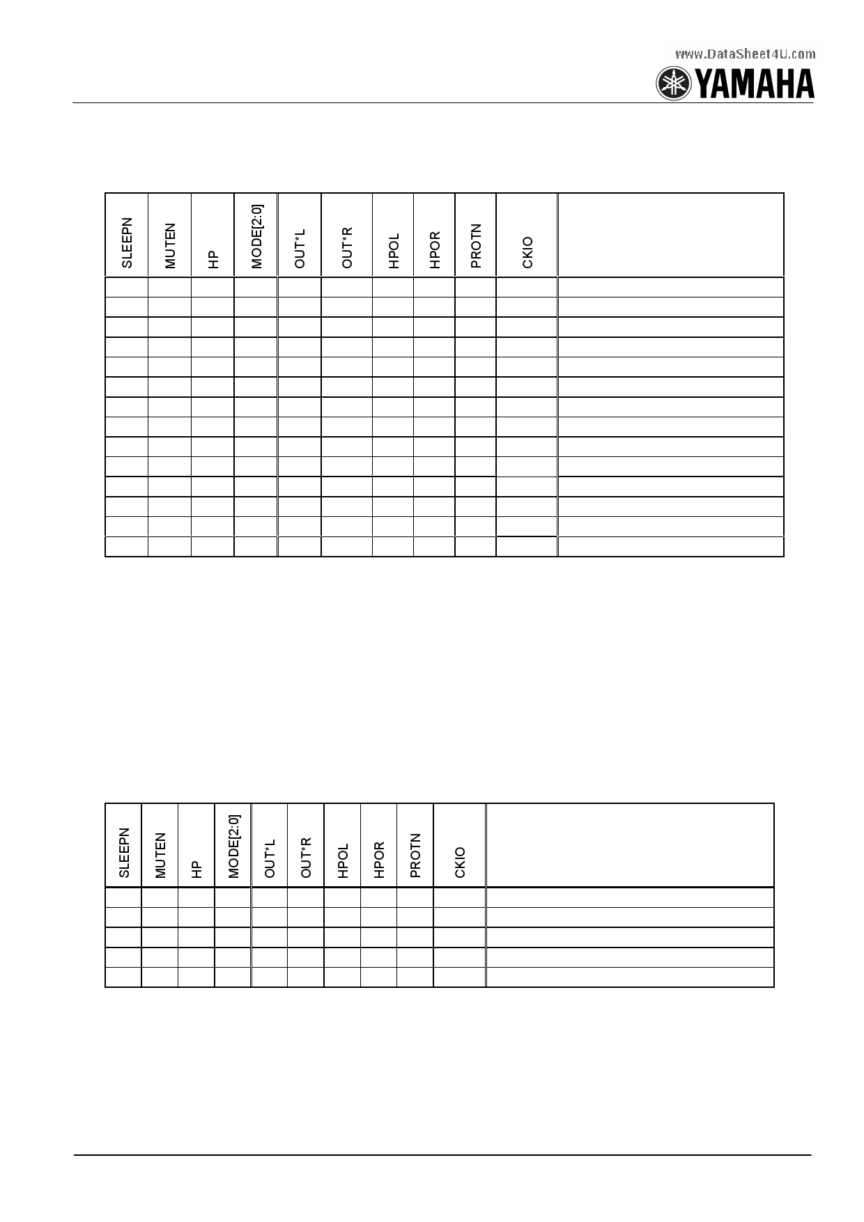
L * * * WL WL WL WL Z
Z Sleep mode
H L L * WL WL WL WL Z
- DA Mute mode *A)
H L H * WL WL RF RF Z
- HA Mute mode *A)
H H L LLL P-H P-H WL WL Z
- DA External Clock Slave mode *A)
H H L LLH P-L P-L WL WL Z
- DA External Clock Slave mode *A)
H H L LHL P-H P-H WL WL Z
- DA External Clock Master mode *A)
H H L LHH P-L P-L WL WL Z
- DA External Clock Master mode *A)
H H L HLL PLS PLS WL WL Z
- DA Internal Clock Slave mode *A)
H H L HHL PLS PLS WL WL Z
- DA Internal Clock Master mode *A)
H H H * WL WL SIG SIG Z
- HA mode *A)
H * * LL* - - - - - CKIN 4.19MHz Clock Input
H * * LH* - - - - - CKOUT 4.19MHz Clock Output
H * * HLL - - - - - CKIN 500kHz Input (Internal Clock)
H * * HHL - - - - - CKOUT 500kHz Output (Internal Clock)
Note:
1) “H” and “L” means logic level High and logic level Low, respectively.
2) “WL” means output disabled (weak pull-down output). “RF” means reference level output. “Z” means Hi-Z.
3) “P-H” means a carrier clock of 524kHz. “P-L” means a carrier clock of 466kHz. “PLS” means a carrier clock of
approx. 500kHz (Internally generated clock).
4) “SIG” means an analog audio signal output.
5) “CKIN” means input of a clock with designated frequency. “CKOUT” means output of a designated clock.
6) “DA” means Digital Amplifier. “HA” means Headphone Amplifier.
7) Each output of OUT*L, OUT*R, HPOL, HPOR, PROTN, and CKIO becomes a state as shown in “Protection
Mode”, depending on the protection state, when entering protection state from a mode except sleep mode.
8) In operating modes indicated by *A), a state of the output signal becomes a state as shown in “Protection Mode”
www.DataSheet4U.cdoumring a protection mode.
9) “HLH” and “HHH” of MODE[2:0] is reserved for system use.
・Protection Mode
Outline
H H L * WL WL WL WL L
Z Digital Amplifier Over-current Protection
H * * * WL WL WL WL L
Z Over-Temperature Protection
H * * * WL WL - - -
- Clock Stop Protection
H * * * WL WL WL WL Z
Z Low Voltage Malfunction Prevention Protection
H H * * WL WL RF RF -
- Power Supply Voltage Fluctuation Protection
Note:
1) Each protection function operates when input terminal is in the designated logic condition. Output terminal
becomes a state as shown in the above during protection mode.
5
5 Page 
YDA143
●Allowable Dissipation
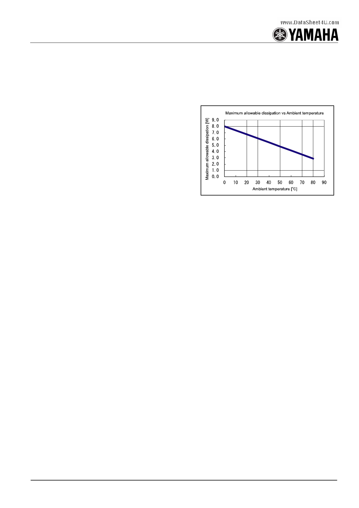
The power dissipation of YDA143 is limited by the junction temperature rating (125℃) and package thermal resistance
(15.6℃/W).
The power dissipation and junction temperature of YDA143 can be found by the following formula.
For the use of YDA143, take care not to exceed the power dissipation and junction temperature.
・Formula for the Power Dissipation
Ploss = (Pout Rpn / Rl) 2 + Idc Vdc
Ploss
Pout
Rpn
Rl
Idc
Vdc
:Allowable Dissipation (W)
:Output Power (W)
:0.39 (Constant)
:Load Resistor (Ω)
:0.040(Constant / at VDDP=12V)
0.030(Constant / at VDDP=9V)
0.045(Constant / at VDDP=13.5V)
:Power supply voltage (V)
・Formula for the junction temperature
Tj = Ploss θja + Ta
Maximum allowable dissipation of YDA143
Ploss
θja
Ta
:Allowable Dissipation (W)
:15.6 (Constant/ package thermal resistance (℃/W))
:Ambient Temperature (℃)
●Package Thermal Resistance
The package (52SSOP) for YDA143 has a Thermal Pad for radiation on the surface. Use this Thermal Pad by soldering on
a board.
The package’s thermal resistance is 15.6℃/W (4-layer board). This thermal resistance is a value measured under the
www.DatafoSlhloeewt4inUg.ccoomnditions: board size 136mm×85mm, 1st layer and 4th layer copper foil board density 154%, 2nd layer and 3rd
layer copper foil board density 200%, no wind. In addition, the lower side pattern of the Thermal Pad is connected to all the
layers in a board by through holes (φ0.4).
11
11 Page | ||
| Páginas | Total 22 Páginas | |
| PDF Descargar | [ Datasheet YDA143.PDF ] | |
Hoja de datos destacado
| Número de pieza | Descripción | Fabricantes |
| YDA142 | DIGITAL INPUT STEREO 9.5W DIGITAL AUDIO POWER AMPLIFIER | YAMAHA CORPORATION |
| YDA143 | STEREO 15W DIGITAL AUDIO POWER AMPLIFIER | YAMAHA CORPORATION |
| YDA144 | STEREO 2.1W Non-Clip DIGITAL AUDIO POWER AMPLIFIER | YAMAHA CORPORATION |
| YDA145 | MONAURAL 2.1W Non-Clip DIGITAL AUDIO POWER AMPLIFIER | YAMAHA CORPORATION |
| Número de pieza | Descripción | Fabricantes |
| SLA6805M | High Voltage 3 phase Motor Driver IC. |
Sanken |
| SDC1742 | 12- and 14-Bit Hybrid Synchro / Resolver-to-Digital Converters. |
Analog Devices |
|
DataSheet.es es una pagina web que funciona como un repositorio de manuales o hoja de datos de muchos de los productos más populares, |
| DataSheet.es | 2020 | Privacy Policy | Contacto | Buscar |
