|
|
|
PDF R2J20602NP Data sheet ( Hoja de datos )
| Número de pieza | R2J20602NP | |
| Descripción | Integrated Driver | |
| Fabricantes | Renesas Technology | |
| Logotipo | ||
Hay una vista previa y un enlace de descarga de R2J20602NP (archivo pdf) en la parte inferior de esta página. Total 15 Páginas | ||
|
No Preview Available !
R2J20602NP
Integrated Driver – MOS FET (DrMOS)
REJ03G1480-0300
Rev.3.00
Jun 30, 2008
Description
The R2J20602NP multi-chip module incorporates a high-side MOS FET, low-side MOS FET, and MOS-FET driver in
a single QFN package. The on and off timing of the power MOS FET is optimized by the built-in driver, making this
device suitable for large-current buck converters. The chip also incorporates a high-side bootstrap Schottky barrier
diode (SBD), eliminating the need for an external SBD for this purpose.
Integrating a driver and both high-side and low-side power MOS FETs, the new device is also compliant with the
package standard “Integrated Driver – MOS FET (DrMOS)” proposed by Intel Corporation.
Features
• Built-in power MOS FET suitable for applications with 12 V input and low output voltage
• Built-in driver circuit which matches the power MOS FET
• Built-in tri-state input function which can support a number of PWM controllers
• VIN operating-voltage range: 16 V max
• High-frequency operation (above 1 MHz) possible
• Large average output current (Max. 40 A)
• Achieve low power dissipation (About 4.4 W at 1 MHz, 25 A)
• Controllable driver: Remote on/off
• Built-in Schottky diode for bootstrapping
• Low-side drive voltage can be independently set
• Small package: QFN56 (8 mm × 8 mm × 0.95 mm)
• Terminal Pb-free
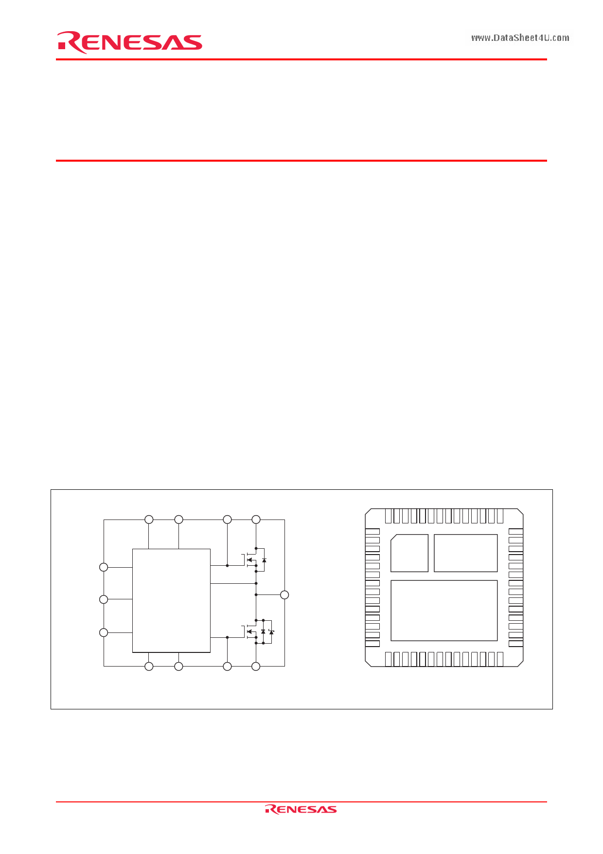
Outline
www.DataSheet4U.com
VCIN BOOT
GH VIN
Reg5V
1 14
56 15
Driver
Tab
High-side MOS
Tab
DISBL#
PWM
MOS FET Driver
VSWH
43
Low-side MOS Tab
28
CGND VLDRV
GL PGND
42 29
(Bottom view)
QFN56 package 8 mm × 8 mm
REJ03G1480-0300 Rev.3.00 Jun 30, 2008
Page 1 of 14
1 page 
R2J20602NP
Electrical Characteristics
(Ta = 25°C, VCIN = 12 V, VLDRV = 5 V, VSWH = 0 V, unless otherwise specified)
Item
Symbol Min Typ Max Units
Test Conditions
Supply
VCIN start threshold
VCIN shutdown threshold
UVLO hysteresis
VCIN bias current
VLDRV bias current
PWM
Input
PWM rising threshold
PWM falling threshold
PWM input resistance
5V
Regulator
Tri-state shutdown window
Shutdown hold-off time
Output voltage
Line regulation
VH
VL
dUVL
ICIN
ILDRV
VH-PWM
VL-PWM
RIN-PWM
VIN-SD
tHOLD-OFF
Vreg
Vreg-line
7.0 7.4 7.8
6.6 7.0 7.4
— 0.4 *1 —
10.5 14.0 18.5
35.5 44.0 52.5
3.7 4.0 4.3
0.9 1.2 1.5
12.5 25 37.5
VL-PWM
—
4.95
–10
—
240 *1
5.2
0
VH-PWM
—
5.45
10
V
V
V VH – VL
mA fPWM = 1 MHz,
ton-PWM = 125 ns
mA fPWM = 1 MHz,
ton-PWM = 125 ns
V
V
kΩ
4V–1V
IPWM (VPWM = 4 V) – IPWM (VPWM = 1 V)
V
ns
V
mV VCIN = 12 V to 16 V
Load regulation
Vreg-load –10
0
10 mV Ireg = 0 to 10 mA
DISBL#
Input
Disable threshold
Enable threshold
VDISBL
VENBL
0.9 1.2 1.5 V
1.9 2.4 2.9 V
Input current
IDISBL
0.5 2.0 5.0 µA DISBL# = 1 V
Note: 1. Reference values for design. Not 100% tested in production.
www.DataSheet4U.com
REJ03G1480-0300 Rev.3.00 Jun 30, 2008
Page 5 of 14
5 Page 
R2J20602NP
The PWM input is TTL level and has hysteresis. When the PWM input signal is abnormal, e.g., when the signal route
from the control IC is abnormal, the tri-state function turns off the high- and low-side MOS FETs. This function
operates when the PWM input signal stays in the input hysteresis window for 240 ns (typ.). After the tri-state mode has
been entered and GH and GL have become low, a PWM input voltage of 4.0 V or more is required to make the circuit
return to normal operation.
240 ns(tHOLD-OFF)
240 ns(tHOLD-OFF)
4.0 V
PWM 1.2 V
GH
GL
4.0 V
PWM 1.2 V
240 ns(tHOLD-OFF)
240 ns(tHOLD-OFF)
GH
GL
www.DataSheet4U.com
Figure 1
For the high-side driver, the BOOT pin is the power-supply voltage pin and voltage VSWH provides a standard for
operation of the high-side driving circuit. Consequently, the difference between the voltage on the BOOT and VSWH
pins becomes the gate swing for the high-side MOS FET. Connect a bootstrap capacitor between the BOOT pin and the
VSWH pin. Since the Schottky barrier diode (SBD) is connected between the BOOT and Reg5V pins, this bootstrap
capacitor is charged up to 5 V. When the high-side MOS FET is turned on, voltage VSWH becomes equal to VIN, so
VBOOT is boosted to VSWH + 5 V.
The GH and GL pins are the gate-monitor pins for each MOS FET.
MOS FETs
The MOS FETs incorporated in R2J20602NP are highly suitable for synchronous-rectification buck conversion. For
the high-side MOS FET, the drain is connected to the VIN pin and the source is connected to the VSWH pin. For the
low-side MOS FET, the drain is connected to the VSWH pin and the source is connected to the PGND pin.
REJ03G1480-0300 Rev.3.00 Jun 30, 2008
Page 11 of 14
11 Page | ||
| Páginas | Total 15 Páginas | |
| PDF Descargar | [ Datasheet R2J20602NP.PDF ] | |
Hoja de datos destacado
| Número de pieza | Descripción | Fabricantes |
| R2J20602NP | Integrated Driver | Renesas Technology |
| Número de pieza | Descripción | Fabricantes |
| SLA6805M | High Voltage 3 phase Motor Driver IC. |
Sanken |
| SDC1742 | 12- and 14-Bit Hybrid Synchro / Resolver-to-Digital Converters. |
Analog Devices |
|
DataSheet.es es una pagina web que funciona como un repositorio de manuales o hoja de datos de muchos de los productos más populares, |
| DataSheet.es | 2020 | Privacy Policy | Contacto | Buscar |