|
|
|
PDF LM5067 Data sheet ( Hoja de datos )
| Número de pieza | LM5067 | |
| Descripción | Negative Hot Swap / Inrush Current Controller | |
| Fabricantes | National Semiconductor | |
| Logotipo | ||
Hay una vista previa y un enlace de descarga de LM5067 (archivo pdf) en la parte inferior de esta página. Total 24 Páginas | ||
|
No Preview Available !
LM5067
September 9, 2009
Negative Hot Swap / Inrush Current Controller with Power
Limiting
General Description
The LM5067 negative hot swap controller provides intelligent
control of the power supply connections during insertion and
removal of circuit cards from a live system backplane or other
“hot” power sources. The LM5067 provides in-rush current
control to limit system voltage droop and transients. The cur-
rent limit and power dissipation in the external series pass N-
Channel MOSFET are programmable, ensuring operation
within the Safe Operating Area (SOA). In addition, the
LM5067 provides circuit protection by monitoring for over-
current and over-voltage conditions. The POWER GOOD
output indicates when the output voltage is close to the input
voltage. The input under-voltage and over-voltage lockout
levels and hysteresis are programmable, as well as the fault
detection time. The LM5067-1 latches off after a fault detec-
tion, while the LM5067-2 automatically attempts restarts at a
fixed duty cycle. The LM5067 is available in a 10 pin MSOP
package and a 14 pin SOIC package.
Features
■ Wide operating range: -9V to -80V
■ In-rush current limit for safe board insertion into live power
sources
■ Programmable maximum power dissipation in the external
pass device
■ Adjustable current limit
■ Circuit breaker function for severe over-current events
■ Adjustable under-voltage lockout (UVLO) and hysteresis
■ Adjustable over-voltage lockout (OVLO) and hysteresis
■ Initial insertion timer allows ringing and transients to
subside after system connection
■ Programmable fault timer avoids nuisance trips
■ Active high open drain POWER GOOD output
■ Available in latched fault and automatic restart versions
Applications
■ Server Backplane Systems
■ In-Rush Current Limiting
■ Solid State Circuit Breaker
■ Transient Voltage Protector
■ Solid State Relay
■ Under-voltage Lock-out
■ Power Good Detector/Indicator
Package
■ MSOP-10
■ SO-14 (Latched Fault Version)
Typical Application
www.DataSheet4U.com
Negative Power Bus In-Rush and Fault Protection
30030901
© 2009 National Semiconductor Corporation 300309
www.national.com
1 page 
Symbol
Current Limit
VCL
tCL
Circuit Breaker
VCB
tCB
Parameter
Threshold voltage
Response time
Threshold voltage
Response time
Power Limit (PWR Pin)
PWRLIM
Power limit sense voltage (SENSE - VEE)
IPWR
Timer (TIMER Pin)
VTMRH
VTMRL
PWR pin current
Upper threshold
Lower threshold
ITIMER
Insertion time current
Sink current, end of insertion time
Fault detection current
Sink current, end of fault time
DCFAULT
Fault Restart Duty Cycle
tFAULT
Fault to GATE low delay
Power Good (PGD Pin)
PGDTH
Threshold measured at OUT - SENSE
PGDVOL
Output low voltage
PGDIOH
Off leakage current
Thermal Resistance (Note 6)
www.DatθaJSAheet4U.comJunction to Ambient
θJC Junction to Case
θJA Junction to Ambient
θJC Junction to Case
Conditions
Min Typ Max Units
SENSE - VEE voltage
44 50 56 mV
SENSE - VEE stepped from 0 mV
to 80 mV
25
µs
SENSE - VEE voltage
SENSE - VEE stepped from 0 mV
to 150 mV, time to GATE low, no
load
70
100 130
0.65 1.0
mV
µs
OUT - SENSE = 24V, RPWR = 75 16.5 22 27.5 mV
kΩ
VPWR = 2.5V
-23 µA
3.76 4 4.16
Restart cycles (LM5067-2)
1.18 1.25 1.32
End of 8th cycle (LM5067-2)
0.3
Re-enable threshold (LM5067-1)
0.3
TIMER pin = 2V
-9.5 -6 -2.5
TIMER pin = 2V
1.2 1.55 1.9
TIMER pin = 2V
-140 -85 -44
0.9 2.5 4.25
LM5067-2
0.5
TIMER pin reaches 4.0V
15
V
V
V
V
µA
mA
µA
µA
%
µs
Decreasing
1.162 1.23 1.285
Increasing, relative to decreasing 1.143 1.25 1.325
threshold
ISINK = 2 mA
VPGD = 80V
60 150
5
V
mV
µA
MSOP package
MSOP package
SO-14 Package
SO-14 Package
94 °C/W
44 °C/W
90 °C/W
27 °C/W
Note 1: Absolute Maximum Ratings indicate limits beyond which damage to the device may occur. Operating Ratings indicate conditions for which the device is
intended to be functional, but do not guarantee specific performance limits. For guaranteed specifications and conditions see the Electrical Characteristics.
Note 2: The human body model is a 100 pF capacitor discharged through a 1.5 kΩ resistor into each pin.
Note 3: Current out of a pin is indicated as a negative value.
Note 4: For detailed information on soldering plastic MSOP package refer to the Packaging Databook available from National Semiconductor Corporation.
Note 5: Maximum continuous current into VCC is limited by power dissipation and die temperature. See the Thermal Considerations section.
Note 6: Tested on a 4 layer JEDEC board with 2 vias under the package. See JEDEC standards JESD51-7 and JESD51-3. See the Thermal Considerations
section.
Note 7: N/C Pins are internally not connected to anything.
5 www.national.com
5 Page 
Functional Description
The LM5067 is designed to control the in-rush current to the
load upon insertion of a circuit card into a live backplane or
other “hot” power source, thereby limiting the voltage sag on
the backplane’s supply voltage, and the dV/dt of the voltage
applied to the load. Effects on other circuits in the system are
minimized, preventing possible unintended resets. During the
system power up, the maximum power dissipation in the se-
ries pass device is limited to a safe value within the device’s
Safe Operating Area (SOA). After the system power up is
complete, the LM5067 monitors the load for excessive cur-
rents due to a fault or short circuit at the load. Limiting the load
current and/or the power in the external MOSFET for an ex-
tended period of time results in the shutdown of the series
pass MOSFET. After a fault event, the LM5067-1 latches off
until the circuit is re-enabled by external control, while the
LM5067-2 automatically restarts with defined timing. The cir-
cuit breaker function quickly switches off the series pass
device upon detection of a severe over-current condition
caused by, e.g. a short circuit at the load. The Power Good
(PGD) output pin indicates when the output voltage is close
to the normal operating value. Programmable under-voltage
lock-out (UVLO) and over-voltage lock-out (OVLO) circuits
shut down the LM5067 when the system input voltage is out-
side the desired operating range. The typical configuration of
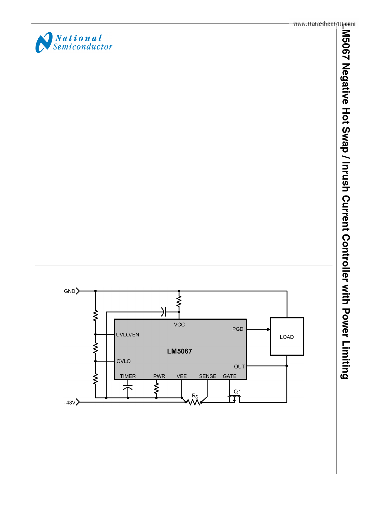
a circuit card with LM5067 hot swap protection is shown in
Figure 2.
FIGURE 2. LM5067 Application
30030929
The LM5067 can be used in a variety of applications, other
than plug-in boards, to monitor for excessive load current,
provide transient protection, and ensuring the voltage to the
load is within preferred limits. The circuit breaker function
protects the system from a sudden short circuit at the load.
Use of the UVLO/EN pin allows the LM5067 to be used as a
solid state relay. The PGD output provides a status indication
of the voltage at the load relative to the input system voltage.
www.DataSheet4U.com
Power Up Sequence
The system voltage range of the LM5067 is -9V to -80V, with
a transient capability to -100V. Referring to the Block Diagram
and Figures 1 and 3, as the system voltage (VSYS) initially
increases from zero, the external N-channel MOSFET (Q1) is
held off by an internal 110 mA pull-down current at the GATE
pin. The strong pull-down current at the GATE pin prevents
an inadvertent turn-on as the MOSFET’s gate-to-drain (Miller)
capacitance is charged. When the operating voltage of the
LM5067 (VCC – VEE) reaches the PORIT threshold (7.7V) the
insertion timer starts. During the insertion time, the capacitor
at the TIMER pin (CT) is charged by a 6 µA current source,
and Q1 is held off by a 2.2 mA pull-down current at the GATE
pin regardless of the system voltage. The insertion time delay
allows ringing and transients at VSYS to settle before Q1 can
be enabled. The insertion time ends when the TIMER pin
voltage reaches 4.0V above VEE, and CT is then quickly dis-
charged by an internal 1.5 mA pull-down current. After the
insertion time, the LM5067 control circuitry is enabled when
the operating voltage reaches the POREN threshold (8.4V).
As VSYS continues to increase, the LM5067 operating voltage
is limited at ≊13V by an internal zener diode. The remainder
of the system voltage is dropped across the input resistor
RIN.
The GATE pin switches on Q1 when VSYS exceeds the UVLO
threshold (UVLO pin >2.5V above VEE). If VSYS exceeds the
UVLO threshold at the end of the insertion time, Q1 is
switched on at that time. The GATE pin sources 52 µA to
charge Q1’s gate capacitance. The maximum gate-to-source
voltage of Q1 is limited by the LM5067’s operating voltage
(VZ) to approximately 13V. During power up, as the voltage
at the OUT pin increases in magnitude with respect to
Ground, the LM5067 monitors Q1’s drain current and power
dissipation. In-rush current limiting and/or power limiting cir-
cuits actively control the current delivered to the load. During
the in-rush limiting interval (t2 in Figure 3) an internal current
source charges CT at the TIMER pin. When the load current
reduces from the limiting value to a value determined by the
load the in-rush limiting interval is complete and CT is dis-
charged. The PGD pin switches high when the voltage at the
OUT pin reaches to within 1.25V of the voltage at the SENSE
pin.
If the TIMER pin voltage reaches 4.0V before in-rush current
limiting or power limiting ceases (during t2), a fault is declared
and Q1 is turned off. See the Fault Timer & Restart section
for a complete description of the fault mode.
11 www.national.com
11 Page | ||
| Páginas | Total 24 Páginas | |
| PDF Descargar | [ Datasheet LM5067.PDF ] | |
Hoja de datos destacado
| Número de pieza | Descripción | Fabricantes |
| LM5060 | LM5060 High-Side Protection Controller with Low Quiescent Current (Rev. G) | Texas Instruments |
| LM5060Q1 | High-Side Protection Controller | National Semiconductor |
| LM5064 | LM5064 Negative Voltage System Pwr Mgmt Protection IC with PMBus (Rev. E) | Texas Instruments |
| LM5066 | LM5066 10 to 80 V Hotswap Controller With I/V/P Monitoring and PMBus Interface (Rev. I) | Texas Instruments |
| Número de pieza | Descripción | Fabricantes |
| SLA6805M | High Voltage 3 phase Motor Driver IC. |
Sanken |
| SDC1742 | 12- and 14-Bit Hybrid Synchro / Resolver-to-Digital Converters. |
Analog Devices |
|
DataSheet.es es una pagina web que funciona como un repositorio de manuales o hoja de datos de muchos de los productos más populares, |
| DataSheet.es | 2020 | Privacy Policy | Contacto | Buscar |