|
|
|
PDF ADF4602 Data sheet ( Hoja de datos )
| Número de pieza | ADF4602 | |
| Descripción | Multiband 3G Femtocell Transceiver | |
| Fabricantes | Analog Devices | |
| Logotipo | ||
Hay una vista previa y un enlace de descarga de ADF4602 (archivo pdf) en la parte inferior de esta página. Total 30 Páginas | ||
|
No Preview Available !
Single-Chip, Multiband 3G Femtocell
Transceiver
ADF4602
FEATURES
Single-chip, multiband 3G transceiver
3GPP 25.104 release 9 WCDMA/HSPA compatible
UMTS band coverage
Local area Class BS in Band I to Band VI and Band VIII to
Band X
Direct conversion transmitter and receiver
Minimal external components
Integrated, multiband, multimode monitoring
No Tx SAW or Rx interstage SAW filters
Integrated power management (3.1 V to 3.6 V supply)
Integrated synthesizers, including PLL loop filters
Integrated PA bias control DACs/GPOs
WCDMA and GSM receive baseband filter options
Easy-to-use with minimal calibration
Automatic Rx DC offset control
Simple gain, frequency, mode programming
Low supply current
50 mA typical Rx current
50 mA to 100 mA Tx current (varies with output power)
6 mm × 6 mm 40-pin LFCSP package
APPLICATIONS
3G home base stations (femtocells)
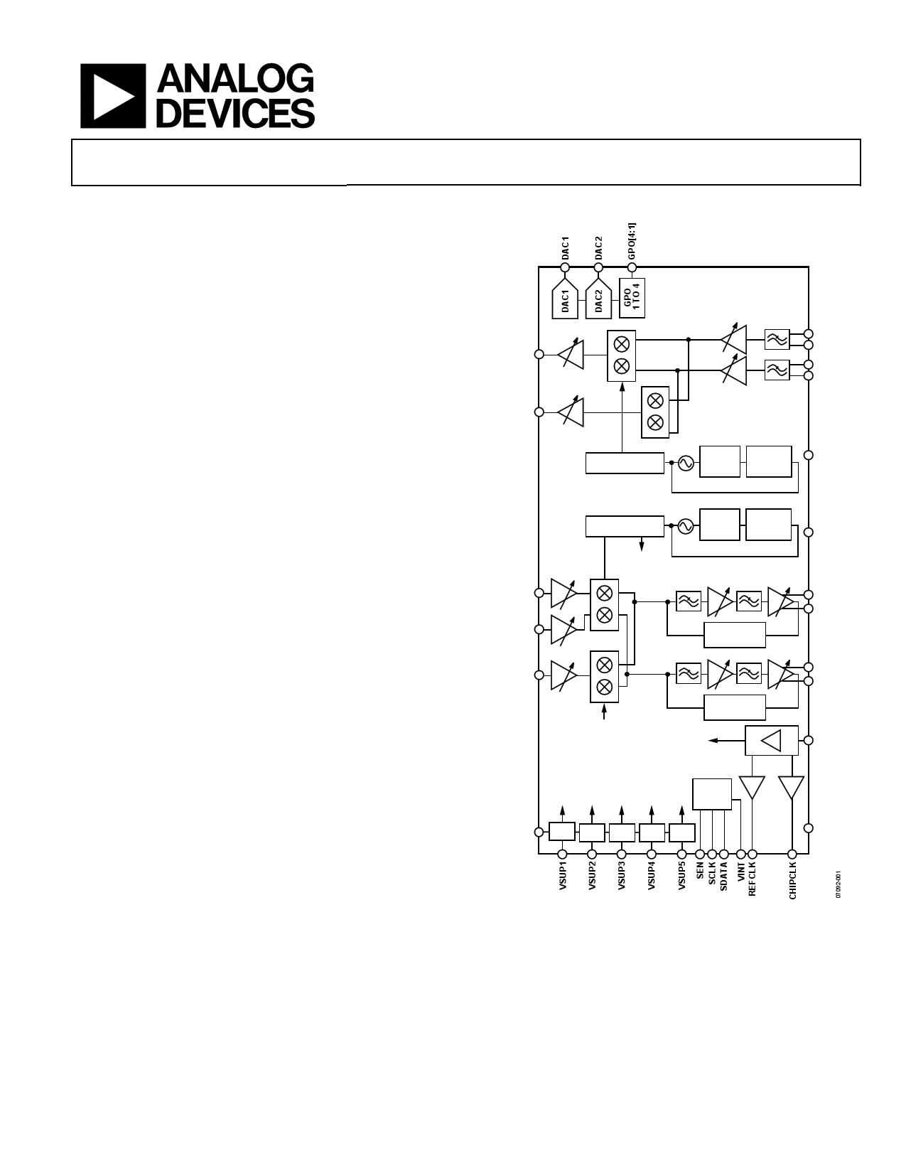
FUNCTIONAL BLOCK DIAGRAM
ADF4602
Tx_PWR_CONTROL
TXLBRF
TXHBRF
Tx_PWR_
CONTROL
Tx_PWR_
CONTROL
LO GENERATOR
Tx_PWR_CONTROL
Tx PLL
LOOP
FILTER
FRAC N
SYNTHE-
SIZER
RXHB1RF
RXHB2RF
LO GENERATOR
Rx PLL
LOOP
FILTER
FRAC N
SYNTHE-
SIZER
Rx_LO_LB
SELECTABLE BANDWIDTH
BASEBAND FILTERS
I
CHAN-
NEL
DC OFFSET
CORRECTION
RXLBRF
Q
CHAN-
NEL
Rx_LO_LB
DC OFFSET
CORRECTION
26MHz 19.2MHz
SERIAL
INTER-
FACE
VDD LDO1 LDO2 LDO3 LDO4 LDO5
TXBBIB
TXBBI
TXBBQ
TXBBQB
VSUP7
VSUP6
RXBBI
RXBBIB
RXBBQ
RXBBQB
REFIN
VSUP8
Figure 1.
Rev. A
Information furnished by Analog Devices is believed to be accurate and reliable. However, no
responsibility is assumed by Analog Devices for its use, nor for any infringements of patents or other
rights of third parties that may result from its use. Specifications subject to change without notice. No
license is granted by implication or otherwise under any patent or patent rights of Analog Devices.
Trademarksandregisteredtrademarksarethepropertyoftheirrespectiveowners.
One Technology Way, P.O. Box 9106, Norwood, MA 02062-9106, U.S.A.
Tel: 781.329.4700
www.analog.com
Fax: 781.461.3113 ©2009–2011 Analog Devices, Inc. All rights reserved.
1 page 
ADF4602
SPECIFICATIONS
VDD = 3.1 V to 3.6 V, GND = 0 V, TA = TMIN to TMAX, unless otherwise noted. Typical specifications are at VDD = 3.3 V and TA = 25°C,
26 MHz reference input level = 0.7 V p-p.
Table 1.
Parameter
REFERENCE SECTION
Reference Input
Reference Input Frequency
Reference Input Amplitude
Reference Input Jitter
REFCLK Output (26 MHz)
Output Load Capacitance
Output Swing
Output Slew Rate
Output Duty Cycle Variation
Output Jitter
CHIPCLK Output (19.2 MHz)
Output Load Capacitance
Frequency Multiplication Ratio
Output Swing
Output Duty Cycle Variation
Output Jitter
Lock Time
TRANSMIT SECTION
I/Q Input
Input Resistance
Input Capacitance
Differential Peak Input Voltage
Input Common-Mode Voltage
Baseband Filter 3 dB Bandwidth
TX Gain Control
Maximum Gain
Gain Control Range
Gain Control Resolution
Gain Control Accuracy
Gain Settling Time
RF Specifications (High Band)
Carrier Frequency
Output Impedance
Output Power (POUT)
Output Noise Spectral Density
Carrier Leakage
FDD EVM
FDD ACLR
Min Typ
Max Unit Test Conditions
0.1
48/65
26
0.7
1.5
10
1.5
200
2
1.5
10
1.5
2
33
50
2.0
40
40
48/65
MHz
V p-p
ps rms
pF
V p-p
V/μs
%
ps rms
pF
N/A
V p-p
%
ps rms
μs
Single-ended operation, dc-coupled1
10 pF load
10 pF load
Input duty cycle = 50%
10 pF load
Input duty cycle = 50%
1.05
1710
100
2
500
1.2
4.0
5
60
1/32
1.0
10
1
50
−8
−155
−161
−161
−163
−35
5
55
70
550
1.4
2170
kΩ
pF
mV pd
V
MHz
Single-ended
Single-ended
dB 1 V p-p differential baseband input
dB
dB Average of LSB steps
dB Any 1 dB step
dB Any 10 dB step
μs POUT within 0.1 dB of final value
MHz
Ω
dBm
dBc/Hz
dBc/Hz
dBc/Hz
dBc/Hz
dBc
%
dB
dB
TM1 signal 64 DPCH
40 MHz offset
80 MHz offset
95 MHz offset
190 MHz offset
POUT = −8 dBm
POUT = −8 dBm
±5 MHz, POUT = −8 dBm
±10 MHz, POUT = −8 dBm
Rev. A | Page 4 of 36
5 Page 
ADF4602
PIN CONFIGURATION AND FUNCTION DESCRIPTIONS
GPO3 1
VSUP1 2
VSUP3 3
RXLBRF 4
NC 5
RXHB2RF 6
RXHB1RF 7
RXBBI 8
RXBBIB 9
RXBBQ 10
PIN 1
INDICATOR
ADF4602
TOP VIEW
(Not to Scale)
30 DAC1
29 DAC2
28 VSUP5
27 TXRFGND
26 TXHBRF
25 TXRFGND
24 TXLBRF
23 TXBBQB
22 TXBBQ
21 VSUP4
NOTES
1. NC = NO CONNECT. DO NOT CONNECT TO THIS PIN.
2. THE EXPOSED PADDLE MUST BE CONNECTED TO GROUND
FOR CORRECT CHIP OPERATION. IT PROVIDES BOTH A
THERMAL AND ELECTRICAL CONNECTION TO THE PCB.
Figure 4. Pin Configuration
Table 4. Pin Function Descriptions
Pin No. Mnemonic
Function
1 GPO3
General Purpose Output 3. Digital output. This is used for external switch or PA control.
2 VSUP11
Output from LDO 1. Supply for receive VCO. Nominal value of 2.6 V. 100 nF decoupling to ground is required.
3 VSUP31
Output from LDO 3. Supply for receive LNA. Nominal value of 1.9 V. 100 nF decoupling to ground is required.
4 RXLBRF
Receive Low Band LNA Input.
5 NC
No Connect. Do not connect to this pin.
6 RXHB2RF
Receive Second High Band LNA Input. Use for UMTS Band II.
7 RXHB1RF
Receive First High Band LNA Input. Use for UMTS Band I.
8 RXBBI
Receive Baseband I Output.
9 RXBBIB
Complementary Receive Baseband I Output.
10 RXBBQ
Receive Baseband Q Output.
11 RXBBQB
Complementary Receive Baseband Q Output.
12 VSUP21
Output from LDO 2. Supply for receive downconverter and baseband. Nominal value of 2.8 V. 100 nF
decoupling to ground is required.
13 VINT
Serial Port Supply Input. 1.8 V should be applied to this pin.
14 SDATA
Serial Port Data Pin. This can be an input or output.
15 SCLK
Serial Clock Input.
16 SEN
Serial Port Enable Input.
17 NC
No Connect. Do not connect to this pin.
18 VSUP71
Transmit Synthesizer Supply Input. Connect to VSUP3 and decouple with 100 nF to ground.
19 TXBBI
Transmit Baseband I Input.
20 TXBBIB
Complementary TX Baseband I Input.
21 VSUP41
Output from LDO4. Supply for transmit VCO. Nominal value of 2.8 V. 100 nF decoupling to GND is required.
22 TXBBQ
Transmit Baseband Q Input.
23 TXBBQB
Complementary TX Baseband Q Input.
24 TXLBRF
Low Band Transmit RF Output. This can output in the range of 824 MHz to 960 MHz.
25 TXRFGND
Transmit RF Ground. Connect this pin to ground.
26 TXHBRF
High Band Transmit RF Output. This can output in the range of 1710 MHz to 2170 MHz.
27 TXRFGND
Transmit RF Ground. Connect this pin to ground.
28 VSUP51
Output from LDO 5. Supply for transmit modulator, baseband, power detector, and DACs. Nominal value of
2.8 V. 100 nF decoupling to ground is required.
29 DAC2
Output from DAC2.
30 DAC1
Output from DAC1.
Rev. A | Page 10 of 36
11 Page | ||
| Páginas | Total 30 Páginas | |
| PDF Descargar | [ Datasheet ADF4602.PDF ] | |
Hoja de datos destacado
| Número de pieza | Descripción | Fabricantes |
| ADF4602 | Multiband 3G Femtocell Transceiver | Analog Devices |
| Número de pieza | Descripción | Fabricantes |
| SLA6805M | High Voltage 3 phase Motor Driver IC. |
Sanken |
| SDC1742 | 12- and 14-Bit Hybrid Synchro / Resolver-to-Digital Converters. |
Analog Devices |
|
DataSheet.es es una pagina web que funciona como un repositorio de manuales o hoja de datos de muchos de los productos más populares, |
| DataSheet.es | 2020 | Privacy Policy | Contacto | Buscar |