|
|
|
PDF TS34119CS Data sheet ( Hoja de datos )
| Número de pieza | TS34119CS | |
| Descripción | Low Power Audio Amplifier | |
| Fabricantes | Taiwan Semiconductor Company | |
| Logotipo | ||
Hay una vista previa y un enlace de descarga de TS34119CS (archivo pdf) en la parte inferior de esta página. Total 11 Páginas | ||
|
No Preview Available !
TS34119
Low Power Audio Amplifier
www.DataSheet4U.com
Supply Voltage Range 2 V to 16V
Gain Adjustable Range 0dB ~ 46dB
Output Power 400mW @Vcc=12V, RL=100Ω
General Description
The TS34119 is a low power audio amplifier, it integrated circuit intended (primarily) for telephone applications, such as
in speakerphones. It provides differential speaker outputs to maximize output swing at low supply voltages (2.0V
minimum). Coupling capacitors to the speaker are not required. Open loop gain is 80dB, and the closed loop gain is set
with two external resistors. A chip Disable pin permits powering down and/or muting the input signal.
The TS34119 is offered in SOP-8 and DIP-8 package.
Features
Ordering Information
Wide operating supply voltage (2~16V)
Chip disable input to power down the IC
Low quiescent current for battery powered application
Lower power down quiescent current
Drives a wide range of speaker load (8~100Ω)
Output power exceed 250mW with 32Ωspeaker
Low total harmonic distortion
Gain adjustable for voice band
Requires few external components
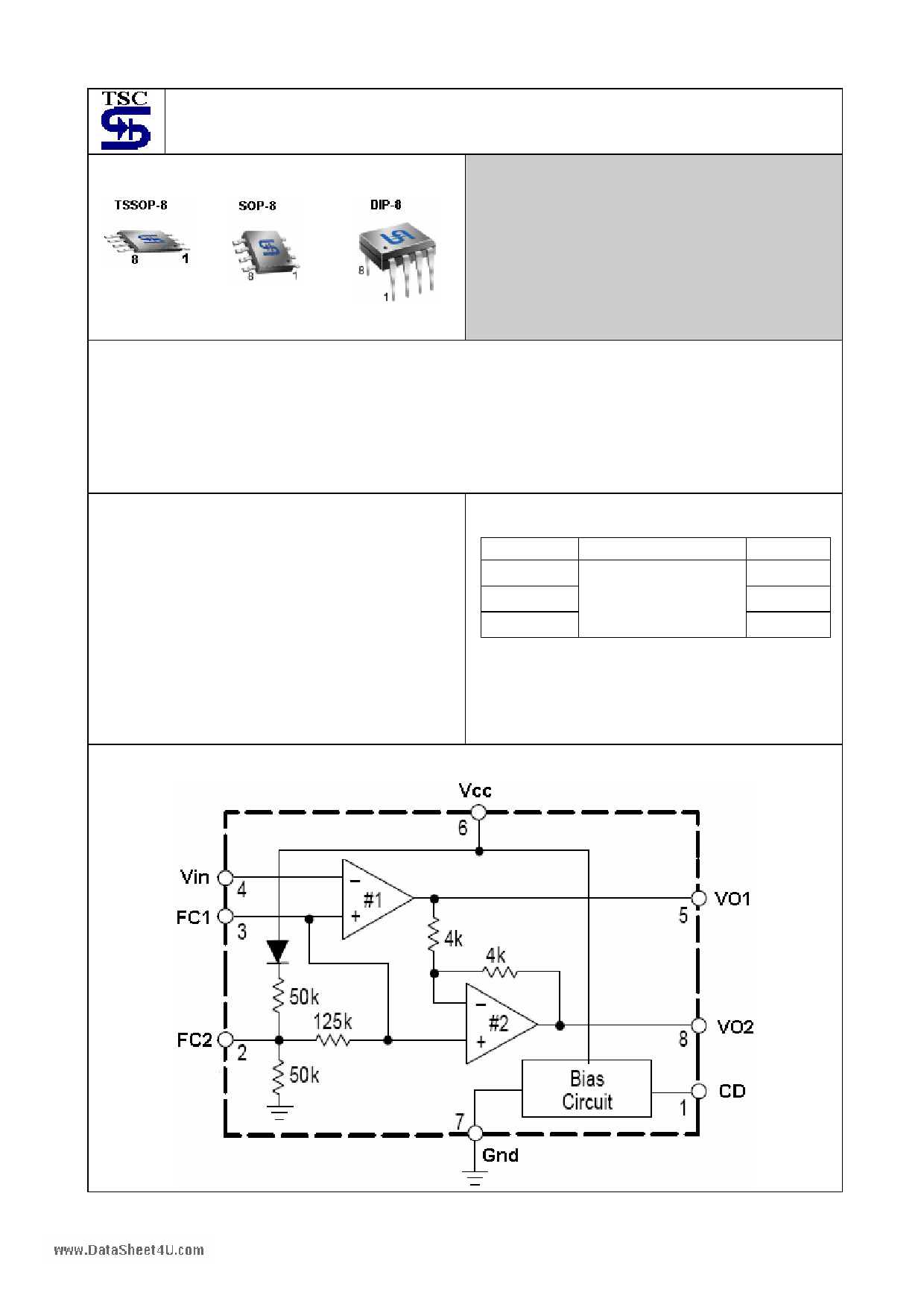
Block Diagram
Part No.
TS34119CD
TS34119CS
TS34119CA
Operating Temp.
-20 ~ +70 oC
Package
DIP-8
SOP-8
TSSOP-8
TS34119
1-11 2004/09 rev. A
1 page 
www.DataSheet4U.com
Design Guideline
GENERAL
The TS34119 is a low power audio amplifier capable of low voltage operation (Vcc=2.0V minimum) such as that
encountered in line-powered speakerphones. The circuit provides a differential output (VO1-VO2) to the speaker to
maximize the available voltage swing at low voltages. The different gain is set by two external resistors. Pins FC1
and FC2 allow controlling the amount of power supply and noise rejection, as well as providing alternate inputs to the
amplifiers. The CD pin permits powering down the IC for muting purposes and to conserve power.
AMPLIFIERS
Referring to the block diagram, the internal configuration consists of two identical operational amplifiers. Amplifier #1
has an open loop gain of ≥80Db (at f≤100Hz), and the closed loop gain is set by external resistor Rf and Rj. The
amplifier is unity gain stable, and has a unity gain frequency of approximately 1.5MHz. In order to adequately cover
the telephone voice band (300Hz to 3.4kHz), a maximum closed loop gain of 46dB is recommended. Amplifier #2 is
internally set to gain of –1.0 (0dB). The outputs of both amplifiers are capable of souring and sinking a peak current
of 200mA.The outputs can typically swing to within ≈ 0.4V above ground, and to within≈1.3V below VCC, at the
maximum current. See Figure 18 and 19 for VOH and VOL curves.
The output dc offset voltage (VO1-VO2) is primarily a function of the feedback resistor (Rf), and secondarily due to
the amplifiers’ input offset voltages. The input offset voltage of the two amplifiers will generally be similar for a
particular IC, and therefore nearly cancel each other at the outputs. Amplifier #1’s bias current, however, flows out of
Vin (pin 4) and through Rf, forcing VO1 to shift negative by an amount equal to (Rf × IIB), Vo2 is shifted posited an
equal amount. The output offset voltage, specified in the Electrical Characteristics is measured with the feedback the
feedback resistor shown in the Typical Application Circuit, and therefore takes into account the bias current as wells
internal offset voltages of the amplifiers. The bias current is constant with respect to VCC.
FC1 AND FC2
Power supply rejection is provided by the capacitors (C1 and C2 in the typical Application Circuit) at FC1 and FC2.
C2 is somewhat dominant at low frequencies, while C1 is dominant at high frequencies, as shown in the graphs of
Figure 4 to 7. The required values of C1 and C2 depend on the conditions of each application. A line powered
speakerphone, for example, will require more filtering than a circuit powered by a well regulated power supply. The
amount of rejection is function of the capacitors, and the equivalent impedance looking into FC1 and FC2 (listed in
the Electrical Characteristics as RFC1 and RFC2). In addition to providing filtering, C1 and C2 also affect the turn-on
time of the circuit at power-up, since the two capacitors must charge up through the internal 50K and 125K resistors.
The graph of Figure 1 indicates the turn-on time upon application of VCC of +6V. The turn-on time is ≈ 60% longer for
VCC =3V, and ≈ 20% less for VCC =9V. Turn-off time is <10uS upon removal of VCC.
CHIP DISABLE
The chip Disable (pin 1) can be used to power down the IC to conserve power, or for muting, or both. When at a
Logic “0” (0V to 0.8V), the TS34119 is enabled for normal operation. When pin 1 is a Logic ”1” (2V to VCC), the IC is
disabled. If pin 1 is open, that is equivalent to Logic “0” although good design proactive dictates that an input should
never be left open. Input impedance at pin 1 is a nominal 90KΩ. The power supply current (when disabled) is shown
in Figure 15.
Muting, defined as the change in differential gain from normal operation to muted operation, is in excess of 70dB.
The turn-off time the audio output, from the application of the CD signal, is <2uS, and turn on-time is 12 mS-15mS.
Both times are independent of C1, C2, and VCC. When the TS34119 is disabled, the voltage at FC1 and FC2 do not
change as they are powered from Vcc. The outputs, VO1 and VO2, change to high impedance condition, removing
the signal from the speaker. If signals from other sources are to be applied to the outputs (while disabled), they must
be within the range of VCC and Ground.
LAYOUT CONSIDERATIONS
Normally a snobbier is not needed at the output of the TS34119, unlike many other audio amplifiers, However, the
PC board layout, stray capacitances, and the manner in which the speaker wires are configured, may dictate
otherwise. Generally, the speaker wires should be twisted tightly, and not more than a few inches in length.
TS34119
5-11 2004/09 rev. A
5 Page 
www.DataSheet4U.com
SOP-8 Mechanical Drawing
A
16 9
BP
18
G
D
CM
K
R
SOP-8 DIMENSION
DIM
MILLIMETERS
MIN MAX
INCHES
MIN MAX
A 4.80
5.00
0.189
0.196
B 3.80
4.00
0.150
0.157
C 1.35
1.75
0.054
0.068
D 0.35
0.49
0.014
0.019
F 0.40
1.25
0.016
0.049
G 1.27 (typ)
0.05 (typ)
K 0.10
M 0o
0.25
7o
0.004
0o
0.009
7o
P 5.80
6.20
0.229
0.244
F
R 0.25
0.50
0.010
0.019
DIP-8 Mechanical Drawing
A
85
B
14
C
K
GD
L
M
DIP-8 DIMENSION
DIM
MILLIMETERS
MIN MAX
INCHES
MIN MAX
A 9.07
9.32
0.357
0.367
B 6.22
6.48
0.245
0.255
C 3.18
4.45
0.125
0.135
D 0.35
0.55
0.019
0.020
G 2.54 (typ)
0.10 (typ)
J 0.29
0.31
0.011
0.012
K 3.25
3.35
0.128
0.132
J
L 7.75
8.00
0.305
0.315
M - 10o - 10o
TS34119
11-11
2004/09 rev. A
11 Page | ||
| Páginas | Total 11 Páginas | |
| PDF Descargar | [ Datasheet TS34119CS.PDF ] | |
Hoja de datos destacado
| Número de pieza | Descripción | Fabricantes |
| TS34119CA | Low Power Audio Amplifier | Taiwan Semiconductor Company |
| TS34119CD | Low Power Audio Amplifier | Taiwan Semiconductor Company |
| TS34119CS | Low Power Audio Amplifier | Taiwan Semiconductor Company |
| Número de pieza | Descripción | Fabricantes |
| SLA6805M | High Voltage 3 phase Motor Driver IC. |
Sanken |
| SDC1742 | 12- and 14-Bit Hybrid Synchro / Resolver-to-Digital Converters. |
Analog Devices |
|
DataSheet.es es una pagina web que funciona como un repositorio de manuales o hoja de datos de muchos de los productos más populares, |
| DataSheet.es | 2020 | Privacy Policy | Contacto | Buscar |