|
|
|
PDF AD6659 Data sheet ( Hoja de datos )
| Número de pieza | AD6659 | |
| Descripción | Dual IF Receiver | |
| Fabricantes | Analog Devices | |
| Logotipo | ||
Hay una vista previa y un enlace de descarga de AD6659 (archivo pdf) en la parte inferior de esta página. Total 30 Páginas | ||
|
No Preview Available !
FEATURES
12-bit, 80 MSPS output data rate per channel
1.8 V analog supply operation (AVDD)
1.8 V to 3.3 V output supply (DRVDD)
Integrated noise shaping requantizer (NSR)
Integrated quadrature error correction (QEC)
Performance with NSR enabled
SNR = 81 dBFS in 16 MHz band up to 30 MHz at 80 MSPS
Performance with NSR disabled
SNR = 72 dBFS up to 70 MHz at 80 MSPS
SFDR = 90 dBc up to 70 MHz input at 80 MSPS
Low power: 98 mW per channel at 80 MSPS
Differential input with 700 MHz bandwidth
On-chip voltage reference and sample-and-hold circuit
2 V p-p differential analog input
Serial port control options
Offset binary, gray code, or twos complement data format
Optional clock duty cycle stabilizer
Integer 1-to-6 input clock divider
Data output multiplex option
Built-in selectable digital test pattern generation
Energy-saving power-down modes
Data clock out with programmable clock and data alignment
APPLICATIONS
Communications
Diversity radio systems
Multimode digital receivers
3G, W-CDMA, LTE, CDMA2000, TD-SCDMA, MC-GSM
I/Q demodulation systems
Smart antenna systems
Battery-powered instruments
General-purpose software radios
www.DataSheet4U.com
Dual IF Receiver
AD6659
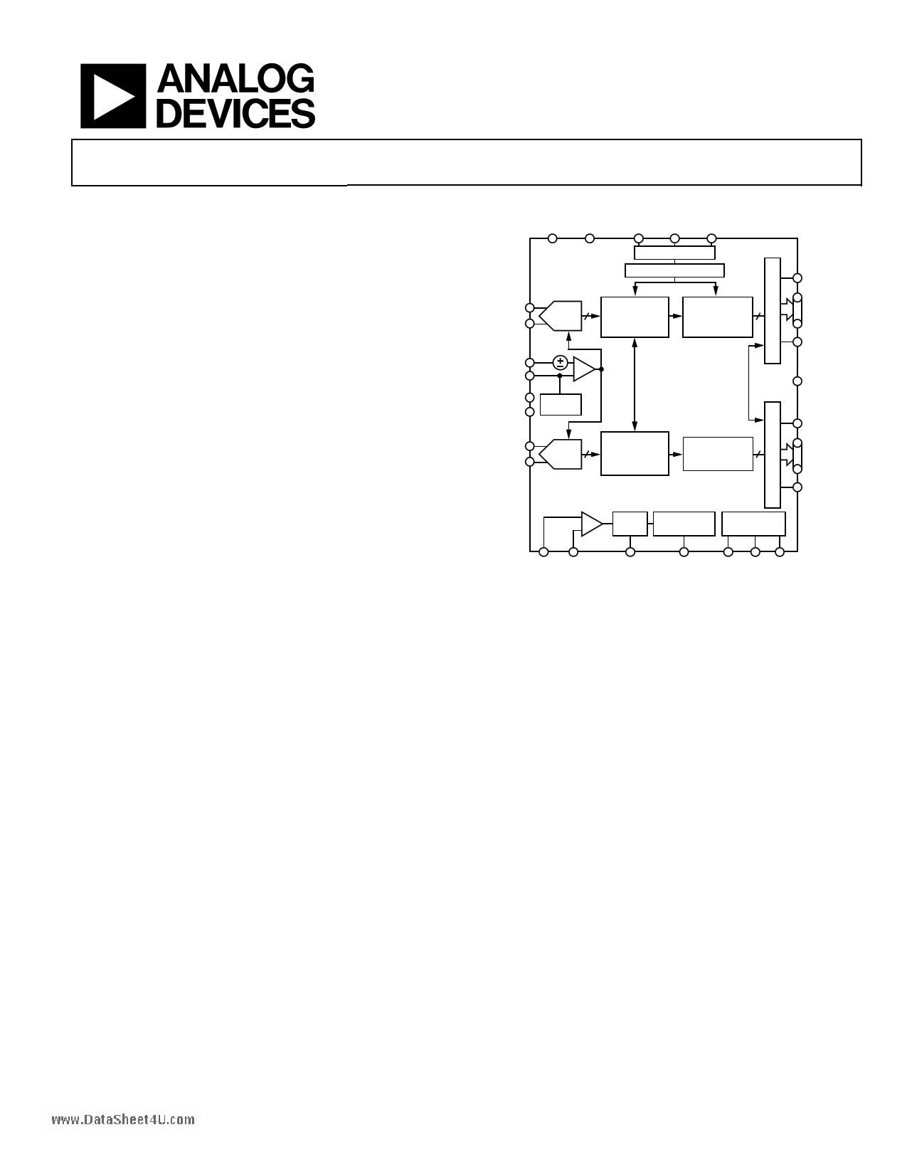
FUNCTIONAL BLOCK DIAGRAM
AVDD AGND
SDIO SCLK CSB
SPI
PROGRAMMING DATA
VIN+A
VIN–A
16
ADC
QUADRATURE
ERROR AND
DC OFFSET
CORRECTION
NOISE
12
SHAPING
REQUANTIZER
VREF
SENSE
VCM
RBIAS
REF
SELECT
AD6659
VIN+B
VIN–B
16
ADC
QUADRATURE
ERROR AND
DC OFFSET
CORRECTION
NOISE
12
SHAPING
REQUANTIZER
ORA
D11A (MSB)
D0A (LSB)
DCOA
DRVDD
ORB
D11B (MSB)
D0B (LSB)
DCOB
DIVIDE DUTY CYCLE
MODE
1 TO 6 STABILIZER CONTROLS
CLK+ CLK–
SYNC
DCS
Figure 1.
PDWN DFS OEB
PRODUCT HIGHLIGHTS
1. The AD6659 operates from a single 1.8 V analog power
supply and features a separate digital output driver supply
to accommodate 1.8 V to 3.3 V logic families.
2. SPI-selectable noise shaping requantizer (NSR) function
that allows for improved SNR within a reduced bandwidth
of up to 70 MHz at 80 MSPS.
3. SPI-selectable dc correction and quadrature error
correction (QEC) that corrects for dc offset, gain, and
phase mismatches between the two channels.
4. A standard serial port interface supports various product
features and functions, such as data output formatting,
internal clock divider, power-down, DCO/data timing,
offset adjustments, and voltage reference modes.
5. The AD6659 is packaged in a 64-lead RoHS-compliant
LFCSP that is pin compatible with the AD9269 16-bit
ADC, the AD9268 16-bit ADC, the AD9258 14-bit ADC,
the AD9251 14-bit ADC, the AD9231 12-bit ADC, and the
AD9204 10-bit ADC, enabling a simple migration path
between 10-bit and 16-bit converters sampling from
20 MSPS to 125 MSPS.
Rev. A
Information furnished by Analog Devices is believed to be accurate and reliable. However, no
responsibility is assumed by Analog Devices for its use, nor for any infringements of patents or other
rights of third parties that may result from its use. Specifications subject to change without notice. No
license is granted by implication or otherwise under any patent or patent rights of Analog Devices.
Trademarksandregisteredtrademarksarethepropertyoftheirrespectiveowners.
One Technology Way, P.O. Box 9106, Norwood, MA 02062-9106, U.S.A.
Tel: 781.329.4700
www.analog.com
Fax: 781.461.3113
©2010 Analog Devices, Inc. All rights reserved.
1 page 
AD6659www.DataSheet4U.com
AC SPECIFICATIONS
AVDD = 1.8 V; DRVDD = 1.8 V, maximum sample rate, 2 V p-p differential input, 1.0 V internal reference; AIN = −1.0 dBFS,
DCS disabled, unless otherwise noted.
Table 2.
Parameter1
SIGNAL-TO-NOISE RATIO (SNR)—NSR DISABLED
fIN = 9.7 MHz
fIN = 30.5 MHz
fIN = 70 MHz
SIGNAL-TO-NOISE RATIO (SNR)—NSR ENABLED
20% Bandwidth (16 MHz @ 80 MSPS)
fIN = 9.7 MHz
fIN = 30.5 MHz
fIN = 70 MHz
SIGNAL-TO-NOISE-AND-DISTORTION (SINAD)
fIN = 9.7 MHz
fIN = 30.5 MHz
fIN = 70 MHz
EFFECTIVE NUMBER OF BITS (ENOB)
fIN = 9.7 MHz
fIN = 30.5 MHz
fIN = 70 MHz
WORST SECOND OR THIRD HARMONIC
fIN = 9.7 MHz
fIN = 30.5 MHz
fIN = 70 MHz
SPURIOUS-FREE DYNAMIC RANGE (SFDR)
fIN = 9.7 MHz
fIN = 30.5 MHz
fIN = 70 MHz
WORST OTHER (HARMONIC OR SPUR)
fIN = 9.7 MHz
fIN = 30.5 MHz
fIN = 70 MHz
TWO-TONE SFDR
fIN = 28.3 MHz (−7 dBFS), 30.6 MHz (−7 dBFS)
CROSSTALK2
ANALOG INPUT BANDWIDTH
Temp
25°C
25°C
25°C
Full
Min Typ
72.4
72.3
72.0
71.4
Max Unit
dBFS
dBFS
dBFS
dBFS
25°C 81.5 dBFS
25°C 81.2 dBFS
25°C 80.3 dBFS
25°C 72.4
25°C 72.2
25°C 71.9
Full 71.5
dBFS
dBFS
dBFS
dBFS
25°C 11.7 Bits
25°C 11.7 Bits
25°C 11.7 Bits
25°C −93 dBc
25°C −92 dBc
25°C −90 dBc
Full −80 dBc
25°C 93
25°C 92
25°C 90
Full 80
dBc
dBc
dBc
dBc
25°C −99 dBc
25°C −99 dBc
25°C −98 dBc
Full −91 dBc
25°C 90
dBc
Full
−110
dBc
25°C 700 MHz
1 See the AN-835 Application Note, Understanding High Speed ADC Testing and Evaluation, for a complete set of definitions.
2 Crosstalk is measured at 100 MHz with −1.0 dBFS on one channel and no input on the alternate channel.
Rev. " | Page 5 of 40
5 Page 
AD6659www.DataSheet4U.com
Pin No.
49, 50, 53, 54, 59, 60, 63, 64
51, 52
55
56
57
58
61, 62
Mnemonic
AVDD
VIN+A, VIN−A
VREF
SENSE
VCM
RBIAS
VIN−B, VIN+B
Description
1.8 V Analog Supply Pins.
Channel A Analog Inputs.
Voltage Reference Input/Output.
Reference Mode Selection.
Analog output voltage at midsupply to set common mode of the analog inputs.
Sets Analog Current Bias. Connect to a 10 kΩ (1% tolerance) resistor to ground.
Channel B Analog Inputs.
Rev. " | Page 11 of 40
11 Page | ||
| Páginas | Total 30 Páginas | |
| PDF Descargar | [ Datasheet AD6659.PDF ] | |
Hoja de datos destacado
| Número de pieza | Descripción | Fabricantes |
| AD6650 | Diversity IF to Baseband GSM/EDGE Narrowband Receiver | Analog Devices |
| AD6652 | 12-Bit / 65 MSPS IF to Baseband Diversity Receiver | Analog Devices |
| AD6653 | IF Diversity Receiver | Analog Devices |
| AD6654 | 4-/6-Channel Wideband IF to Baseband Receiver | Analog Devices |
| Número de pieza | Descripción | Fabricantes |
| SLA6805M | High Voltage 3 phase Motor Driver IC. |
Sanken |
| SDC1742 | 12- and 14-Bit Hybrid Synchro / Resolver-to-Digital Converters. |
Analog Devices |
|
DataSheet.es es una pagina web que funciona como un repositorio de manuales o hoja de datos de muchos de los productos más populares, |
| DataSheet.es | 2020 | Privacy Policy | Contacto | Buscar |