|
|
PDF WED3C755E8M-XBX Data sheet ( Hoja de datos )
| Número de pieza | WED3C755E8M-XBX | |
| Descripción | RISC MICROPROCESSOR MULTI-CHIP PACKAGE | |
| Fabricantes | White Electronic Designs Corporation | |
| Logotipo |  |
|
Hay una vista previa y un enlace de descarga de WED3C755E8M-XBX (archivo pdf) en la parte inferior de esta página. Total 14 Páginas | ||
|
No Preview Available !
White Electronic Designs
www.DataSheet4U.com
WED3C755E8M-XBX
RISC MICROPROCESSOR MULTI-CHIP PACKAGE
OVERVIEW
The WEDC 755E/SSRAM multichip package is targeted
for high performance, space sensitive, low power systems
and supports the following power management features:
doze, nap, sleep and dynamic power management. The
WED3C755E8M-XBX multichip package consists of:
755 RISC processor (E die revision)
Dedicated 1MB SSRAM L2 cache, configured as
128Kx72
21mmx25mm, 255 Ceramic Ball Grid Array (CBGA)
Core Frequency/L2 Cache Frequency (300MHz/
150MHz, 350MHz/175MHz)
Maximum 60x Bus frequency = 66MHz
FEATURES
The WED3C755E8M-XBX is offered in Commercial
(0°C to +70°C), industrial (-40°C to +85°C) and military
(-55°C to +125°C) temperature ranges and is well suited
for embedded applications such as missiles, aerospace,
flight computers, fire control systems and rugged critical
systems.
Footprint compatible with WED3C7558M-XBX and
WED3C750A8M-200BX
Footprint compatible with Motorola MPC 745
This product is subject to change without notice.
FIG. 1 - MULTI-CHIP PACKAGE DIAGRAM
µP
755E
SSRAM
SSRAM
White Electronic Designs Corp. reserves the right to change products or specifications without notice.
May, 2003
Rev 2
1 White Electronic Designs Corporation • (602) 437-1520 • www.wedc.com
1 page 
White Electronic Designs
www.DataSheet4U.com
WED3C755E8M-XBX
Signal Name
A[0-31]
AACK#
ABB#
AP[0-3]
ARTRY#
AVCC
BG#
BR#
BVSEL (4, 5, 6)
CI#
CKSTP_IN#
CKSTP_OUT#
CLK_OUT
DBB#
DBG#
DBDIS#
DBWO#
DH[0-31]
DL[0-31]
DP[0-7]
DRTRY#
GBL#
GND
HRESET#
INT#
L1_TSTCLK (1)
L2_TSTCLK (1)
L2AVCC (8)
L2OVCC
L2VSEL (4, 5, 6, 7)
LSSD_MODE# (1)
MCP#
NC (No-connect)
OVCC (2)
PLL_CFG[0-3]
QACK#
QREQ#
RSRV#
SMI#
SRESET#
STCK (9)
STDI
STDO
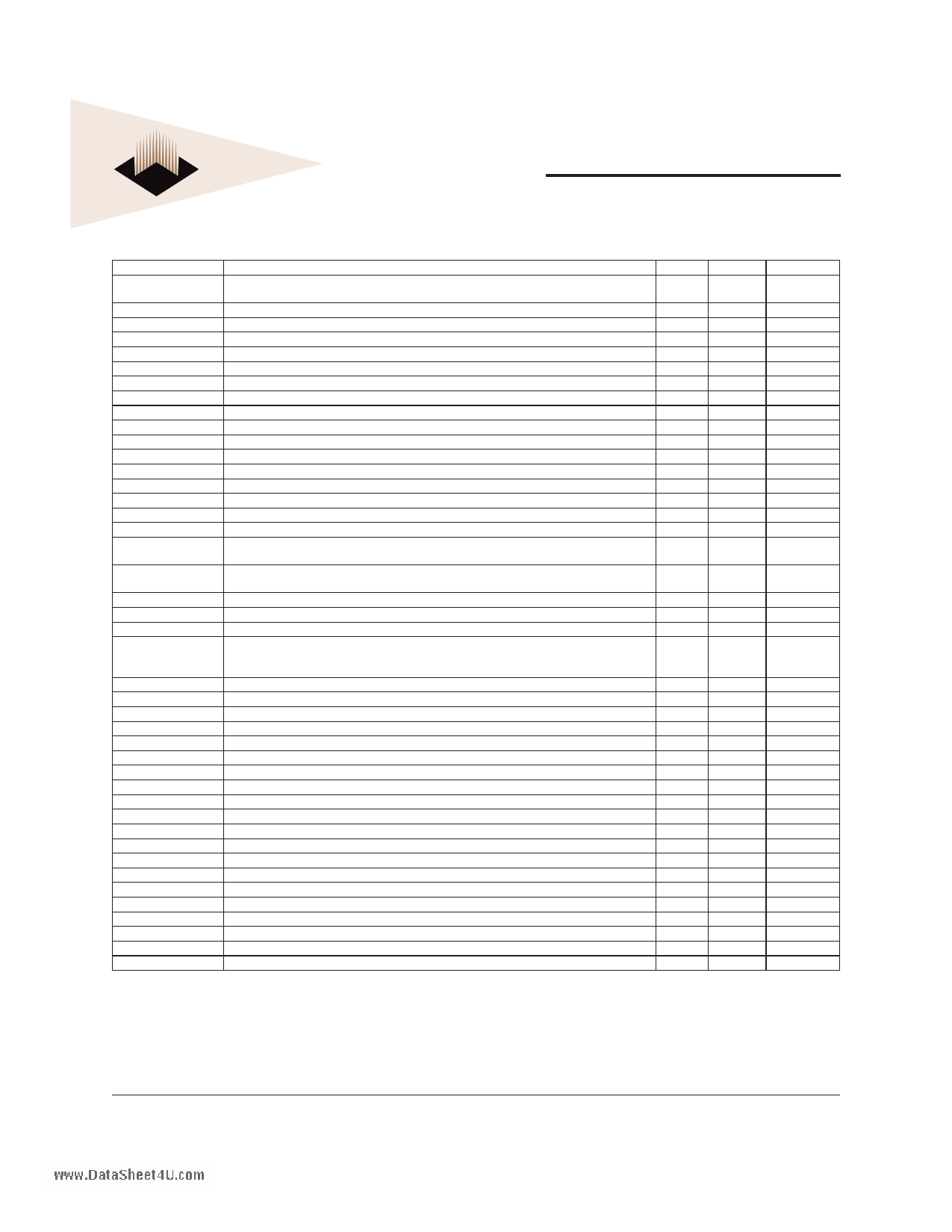
PACKAGE PINOUT LISTING
Pin Number
C16, E4, D13, F2, D14, G1, D15, E2, D16, D4, E13, G2, E15, H1, E16, H2, F13, J1,
F14, J2, F15, H3, F16, F4, G13, K1, G15, K2, H16, M1, J15, P1
L2
K4
C1, B4, B3, B2
J4
A10
L1
B6
B1
E1
D8
A6
D7
J14
N1
H15
G4
P14, T16, R15, T15, R13, R12, P11, N11, R11, T12, T11, R10, P9, N9, T10, R9, T9, P8,
N8, R8, T8, N7, R7, T7, P6, N6, R6, T6, R5, N5, T5, T4
K13, K15, K16, L16, L15, L13, L14, M16, M15, M13, N16, N15, N13, N14, P16, P15,
R16, R14, T14, N10, P13, N12, T13, P3, N3, N4, R3, T1, T2, P4, T3, R4
M2, L3, N2, L4, R1, P2, M4, R2
G16
F1
C5, C12, E3, E6, E8, E9, E11, E14, F5, F7, F10, F12, G6, G8, G9, G11, H5, H7, H10,
H12, J5, J7, J10, J12, K6, K8, K9, K11, L5, L7, L10, L12, M3, M6, M8, M9, M11, M14,
P5, P12
A7
B15
D11
D12
L11
E10, E12, M12, G12, G14, K12, K14
B5
B10
C13
C3, C6, D5, D6, H4, A4, A5, A2, A3
C7, E5, G3, G5, K3, K5, P7, P10, E7, M5, M7, M10
A8, B9, A9, D9
D3
J3
D1
A16
B14
B7
C8
J16
Active
High
Low
Low
High
Low
—
Low
Low
High
Low
Low
Low
—
Low
Low
Low
Low
High
High
High
Low
Low
—
Low
Low
High
High
—
—
High
Low
Low
—
—
High
Low
Low
Low
Low
Low
—
—
—
I/O
I/O
Input
I/O
I/O
I/O
—
Input
Output
Input
Output
Input
Ouput
Output
I/O
Input
Input
Input
I/O
I/O
I/O
Input
I/O
—
Input
Input
Input
Input
—
—
Input
Input
Input
—
—
Input
Input
Output
Output
Input
Input
Input
Input
Output
I/F Voltage
OVCC
OVCC
OVCC
OVCC
OVCC
2.0V
OVCC
OVCC
OVCC
OVCC
OVCC
OVCC
OVCC
OVCC
OVCC
OVCC
OVCC
OVCC
OVCC
OVCC
OVCC
OVCC
GND
OVCC
OVCC
—
—
2.0V
L20VCC
L20VCC
—
OVCC
—
OVCC
OVCC
OVCC
OVCC
OVCC
OVCC
OVCC
L20VCC
L20VCC
L20VCC
White Electronic Designs Corp. reserves the right to change products or specifications without notice.
May, 2003
Rev 2
5 White Electronic Designs Corporation • (602) 437-1520 • www.wedc.com
5 Page 
White Electronic Designs
www.DataSheet4U.com
WED3C755E8M-XBX
PLL POWER SUPPLY FILTERING
The AVCC and L2AVCC power signals are provided on
the WED3C755E8M-XBX to provide power to the clock
generation phase-locked loop and L2 cache delay-locked
loop respectively. To ensure stability of the internal clock,
the power supplied to the AVCC input signal should be
filtered of any noise in the 500kHz to 10 MHz resonant
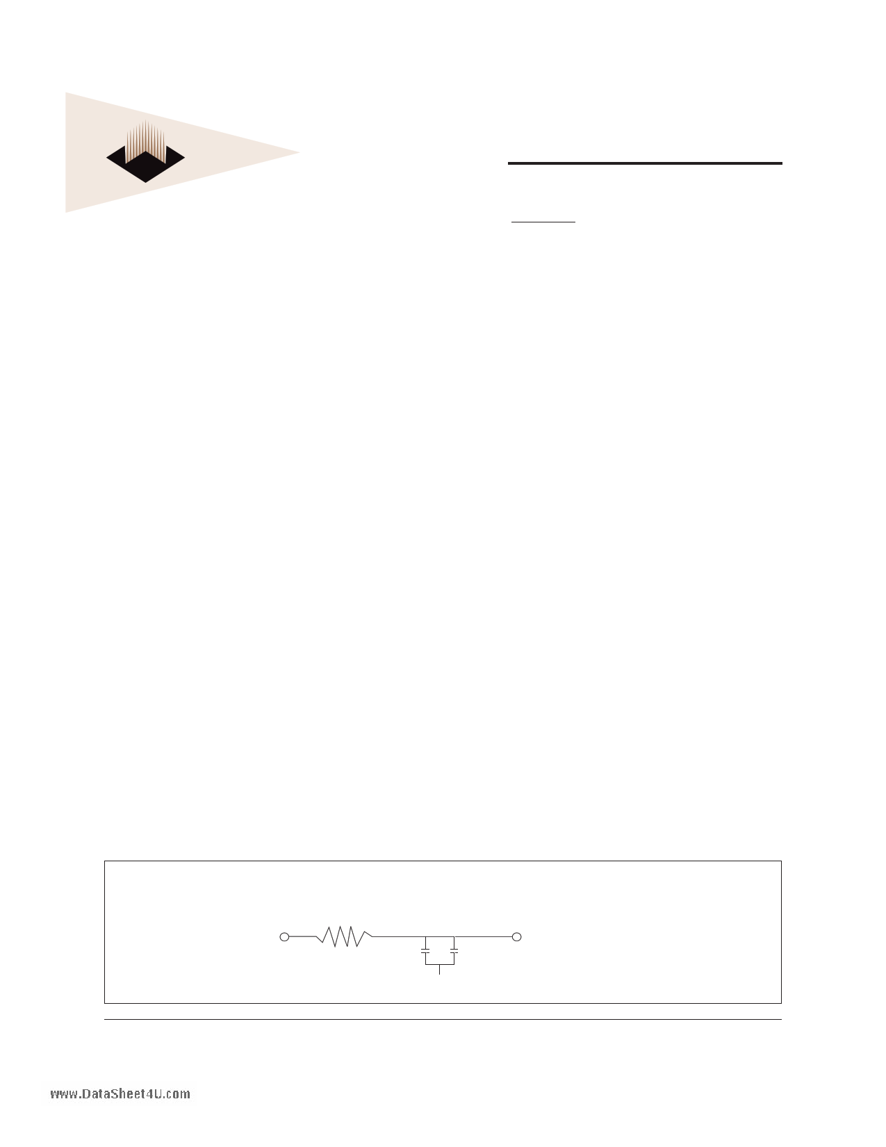
frequency range of the PLL. A circuit similar to the
one shown in Figure 6 using surface mount capacitors
with minimum Effective Series Inductance (ESL) is
recommended. Multiple small capacitors of equal value
are recommended over a single large value capacitor.
The circuit should be placed as close as possible to the
AVCC pin to minimize noise coupled from nearby circuits.
An identical but separate circuit should be placed as close
as possible to the L2AVCC pin. It is often possible to route
directly from the capacitors to the AVCC pin, which is on the
periphery of the 255 BGA footprint, without the inductance
of vias. The L2AVCC pin may be more difficult to route but
is proportionately less critical.
PULL-UP RESISTOR REQUIREMENTS
The WED3C755E8M-XBX requires pull-up resistors (1
kW-5 kW) on several control pins of the bus interface to
maintain the control signals in the negated state after they
have been actively negated and released by the processor
or other bus masters. These pins are TS#, ABB#, AACK#,
ARTRY#, DBB#, DBWO#, TA#, TEA#, and DBDIS#.
DRTRY# should also be connected to a pull-up resistor
(1 kW-5 kW) if it will be used by the system; otherwise,
this signal should be connected to HRESET# to select
NO-DRTRY mode.
Three test pins also require pull-up resistors (100 W-1 kW).
These pins are L1_TSTCLK, L2_TSTCLK, and LSSD_
MODE#. These signals are for factory use only and must
be pulled up to OVCC for normal machine operation.
In addition, CKSTP_OUT# is an open-drain style output
that requires a pull-up resistor (1 kW-5 kW) if it is used by
the system. During inactive periods on the bus, the address
and transfer attributes may not be driven by any master
and may, therefore, float in the high-impedance state for
relatively long periods of time. Since the processor must
continually monitor these signals for snooping, this float
condition may cause additional power draw by the input
receivers on the processor or by other receivers in the
system. These signals can be pulled up through weak (10
kW) pull-up resistors by the system or may be otherwise
driven by the system during inactive periods of the bus to
avoid this additional power draw, but address bus pull-up
resistors are not neccessary for proper device operation.
The snooped address and transfer attribute inputs are:
A[0:31], AP[0:3], TT[0:4], TBST#, and GBL#.
The data bus input receivers are normally turned off
when no read operation is in progress and, therefore, do
not require pull-up resistors on the bus. Other data bus
receivers in the system, however, may require pull-ups, or
that those signals be otherwise driven by the system during
inactive periods by the system. The data bus signals are:
DH[0:31], DL[0:31], and DP[0:7].
If 32-bit data bus mode is selected, the input receivers of
the unused data and parity bits will be disabled, and their
outputs will drive logic zeros when they would otherwise
normally be driven. For this mode, these pins do not require
pull-up resistors, and should be left unconnected by the
system to minimize possible output switching.
If address or data parity is not used by the system, and
the respective parity checking is disabled through HID0,
the input receivers for those pins are disabled, and those
pins do not require pull-up resistors and should be left
unconnected by the system. If all parity generation is
disabled through HID0, then all parity checking should
also be disabled through HID0, and all parity pins may be
left unconnected by the system.
FIG. 6 - POWER SUPPLY FILTER CIRCUIT
VCC
10 Ω
2.2 µF
2.2 µF
AVCC (or L2AVCC)
Low ESL surface mount capacitors
GND
White Electronic Designs Corp. reserves the right to change products or specifications without notice.
May, 2003
Rev 2
11 White Electronic Designs Corporation • (602) 437-1520 • www.wedc.com
11 Page | ||
| Páginas | Total 14 Páginas | |
| PDF Descargar | [ Datasheet WED3C755E8M-XBX.PDF ] | |
Hoja de datos destacado
| Número de pieza | Descripción | Fabricantes |
| WED3C755E8M-XBX | RISC MICROPROCESSOR MULTI-CHIP PACKAGE | White Electronic Designs Corporation |
| Número de pieza | Descripción | Fabricantes |
| SLA6805M | High Voltage 3 phase Motor Driver IC. |
Sanken |
| SDC1742 | 12- and 14-Bit Hybrid Synchro / Resolver-to-Digital Converters. |
Analog Devices |
|
DataSheet.es es una pagina web que funciona como un repositorio de manuales o hoja de datos de muchos de los productos más populares, |
| DataSheet.es | 2020 | Privacy Policy | Contacto | Buscar |
