|
|
|
PDF LM4951 Data sheet ( Hoja de datos )
| Número de pieza | LM4951 | |
| Descripción | Wide Voltage Range 1.8 Watt Audio Amplifier | |
| Fabricantes | National Semiconductor | |
| Logotipo | ||
Hay una vista previa y un enlace de descarga de LM4951 (archivo pdf) en la parte inferior de esta página. Total 18 Páginas | ||
|
No Preview Available !
November 2005
www.DataSheet4U.com
LM4951
Wide Voltage Range 1.8 Watt Audio Amplifier
General Description
The LM4951 is an audio power amplifier primarily designed
for demanding applications in Portable Handheld devices. It
is capable of delivering 1.8W mono BTL to an 8Ω load,
continuous average power, with less than 1% distortion
(THD+N) from a 7.5VDC power supply.
Boomer audio power amplifiers were designed specifically to
provide high quality output power with a minimal amount of
external components. The LM4951 does not require boot-
strap capacitors, or snubber circuits.
The LM4951 features a low-power consumption active-low
shutdown mode. Additionally, the LM4951 features an inter-
nal thermal shutdown protection mechanism.
The LM4951 contains advanced pop & click circuitry that
eliminates noises which would otherwise occur during
turn-on and turn-off transitions.
The LM4951 is unity-gain stable and can be configured by
external gain-setting resistors.
Key Specifications
j Wide Voltage Range
j Quiescent Power Supply Current
(VDD = 7.5V)
j Power Output BTL at 7.5V,
1% THD
j Shutdown Current
j Fast Turn on Time
2.7V to 9V
2.5mA (typ)
1.8W (typ)
0.01µA (typ)
25mS (typ)
Features
n Pop & click circuitry eliminates noise during turn-on and
turn-off transitions
n Low current, active-low shutdown mode
n Low quiescent current
n Thermal shutdown protection
n Unity-gain stable
n External gain configuration capability
Applications
n Portable Handheld Devices up to 9V
n Cell Phone
n PDA
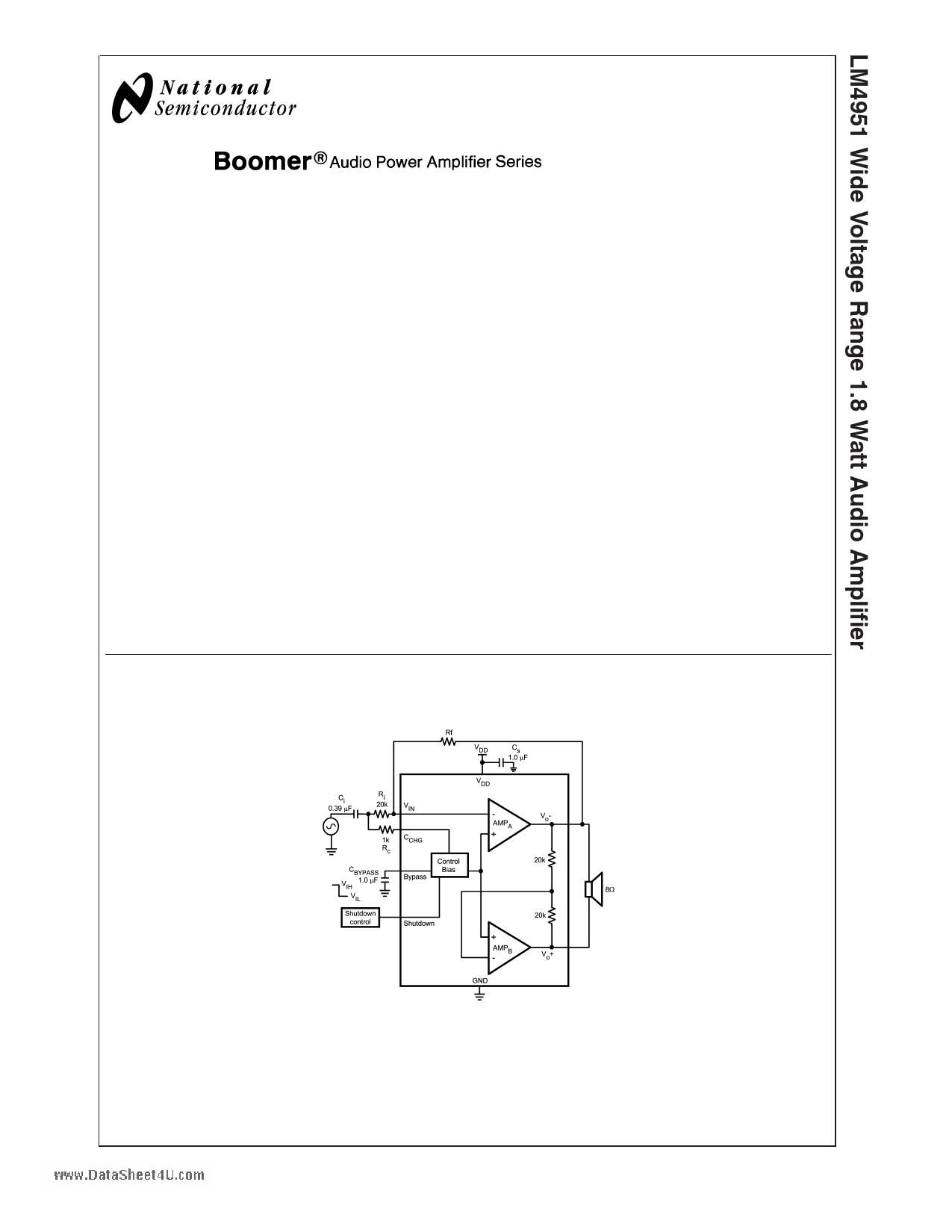
Typical Application
200942F4
* RC is needed for over/under voltage protection. If inputs are less than VDD +0.3V and greater than –0.3V, and if inputs are
disabled when in shutdown mode, then RC may be shorted.
FIGURE 1. Typical Bridge-Tied-Load (BTL) Audio Amplifier Application Circuit
Boomer® is a registered trademark of National Semiconductor Corporation.
© 2005 National Semiconductor Corporation DS200942
www.national.com
1 page 
Typical Performance Characteristics
THD+N vs Frequency
VDD = 3.3V, PO = 100mW, AV = 6dB
www.DataSheet4U.com
THD+N vs Frequency
VDD = 3.3V, PO = 100mW, AV = 26dB
200942F9
THD+N vs Frequency
VDD = 5V, PO = 400mW, AV = 6dB
20094202
THD+N vs Frequency
VDD = 5V, PO = 400mW, AV = 26dB
20094203
THD+N vs Frequency
VDD = 7.5V, PO = 600mW, AV = 6dB
20094204
THD+N vs Frequency
VDD = 7.5V, PO = 600mW, AV = 26dB
20094205
5
200942G0
www.national.com
5 Page 
Application Information
HIGH VOLTAGE BOOMER
Unlike previous 5V Boomer® amplifiers, the LM4951 is de-
signed to operate over a power supply voltages range of
2.7V to 9V. Operating on a 7.5V power supply, the LM4951
will deliver 1.8W into an 8Ω BTL load with no more than 1%
THD+N.
BRIDGE CONFIGURATION EXPLANATION
As shown in Figure 1, the LM4951 consists of two opera-
tional amplifiers that drive a speaker connected between
their outputs. The value of input and feedback resistors
determine the gain of each amplifier. External resistors Ri
and Rf set the closed-loop gain of AMPA, whereas two 20kΩ
internal resistors set AMPB’s gain to -1. The LM4951 drives
a load, such as a speaker, connected between the two
amplifier outputs, VO+ and VO -. Figure 1 shows that AMPA’s
output serves as AMPB’s input. This results in both amplifiers
producing signals identical in magnitude, but 180˚ out of
phase. Taking advantage of this phase difference, a load is
placed between AMPA and AMPB and driven differentially
(commonly referred to as "bridge mode"). This results in a
differential, or BTL, gain of
PDMAX’ = (TJMAX - TA) / θJAwww.DataShe(3e)t4U.com
The LM4951’s TJMAX = 150˚C. In the SD package, the
LM4951’s θJA is 73˚C/W when the metal tab is soldered to a
copper plane of at least 1in2. This plane can be split between
the top and bottom layers of a two-sided PCB. Connect the
two layers together under the tab with an array of vias. At any
given ambient temperature TA, use Equation (3) to find the
maximum internal power dissipation supported by the IC
packaging. Rearranging Equation (3) and substituting PDMAX
for PDMAX’ results in Equation (4). This equation gives the
maximum ambient temperature that still allows maximum
stereo power dissipation without violating the LM4951’s
maximum junction temperature.
TA = TJMAX - PDMAX-MONOBTLθJA
(4)
For a typical application with a 7.5V power supply and a BTL
8Ω load, the maximum ambient temperature that allows
maximum stereo power dissipation without exceeding the
maximum junction temperature is approximately 46˚C for the
TS package.
AVD = 2(Rf / Ri)
(1)
Bridge mode amplifiers are different from single-ended am-
plifiers that drive loads connected between a single amplifi-
er’s output and ground. For a given supply voltage, bridge
mode has a distinct advantage over the single-ended con-
figuration: its differential output doubles the voltage swing
across the load. Theoretically, this produces four times the
output power when compared to a single-ended amplifier
under the same conditions. This increase in attainable output
power assumes that the amplifier is not current limited and
that the output signal is not clipped. To ensure minimum
output signal clipping when choosing an amplifier’s closed-
loop gain, refer to the AUDIO POWER AMPLIFIER DESIGN
section. Under rare conditions, with unique combinations of
high power supply voltage and high closed loop gain set-
tings, the LM4951 may exhibit low frequency oscillations.
Another advantage of the differential bridge output is no net
DC voltage across the load. This is accomplished by biasing
AMP1’s and AMP2’s outputs at half-supply. This eliminates
the coupling capacitor that single supply, single-ended am-
plifiers require. Eliminating an output coupling capacitor in a
typical single-ended configuration forces a single-supply am-
plifier’s half-supply bias voltage across the load. This in-
creases internal IC power dissipation and may permanently
damage loads such as speakers.
POWER DISSIPATION
Power dissipation is a major concern when designing a
successful bridged amplifier.
The LM4951’s dissipation when driving a BTL load is given
by Equation (2). For a 7.5V supply and a single 8Ω BTL load,
the dissipation is 1.42W.
PDMAX-MONOBTL = 4(VDD) 2 / 2π2RL: Bridge Mode (2)
The maximum power dissipation point given by Equation (2)
must not exceed the power dissipation given by Equation
(3):
TJMAX = PDMAX-MONOBTLθJA + TA
(5)
Equation (5) gives the maximum junction temperature
TJMAX. If the result violates the LM4951’s 150˚C, reduce the
maximum junction temperature by reducing the power sup-
ply voltage or increasing the load resistance. Further allow-
ance should be made for increased ambient temperatures.
The above examples assume that a device is operating
around the maximum power dissipation point. Since internal
power dissipation is a function of output power, higher am-
bient temperatures are allowed as output power or duty
cycle decreases.
If the result of Equation (2) is greater than that of Equation
(3), then decrease the supply voltage, increase the load
impedance, or reduce the ambient temperature. Further,
ensure that speakers rated at a nominal 8Ω do not fall below
6Ω. If these measures are insufficient, a heat sink can be
added to reduce θJA. The heat sink can be created using
additional copper area around the package, with connec-
tions to the ground pins, supply pin and amplifier output pins.
Refer to the Typical Performance Characteristics curves
for power dissipation information at lower output power lev-
els.
POWER SUPPLY VOLTAGE LIMITS
Continuous proper operation is ensured by never exceeding
the voltage applied to any pin, with respect to ground, as
listed in the Absolute Maximum Ratings section.
POWER SUPPLY BYPASSING
As with any power amplifier, proper supply bypassing is
critical for low noise performance and high power supply
rejection. Applications that employ a voltage regulator typi-
cally use a 10µF in parallel with a 0.1µF filter capacitors to
stabilize the regulator’s output, reduce noise on the supply
line, and improve the supply’s transient response. However,
their presence does not eliminate the need for a local 1.0µF
tantalum bypass capacitance connected between the
LM4951’s supply pins and ground. Do not substitute a ce-
ramic capacitor for the tantalum. Doing so may cause oscil-
11 www.national.com
11 Page | ||
| Páginas | Total 18 Páginas | |
| PDF Descargar | [ Datasheet LM4951.PDF ] | |
Hoja de datos destacado
| Número de pieza | Descripción | Fabricantes |
| LM4950 | 7.5W Mono-BTL or 3.1W Stereo Audio Power Amplifier | National Semiconductor |
| LM4950 | LM4950 7.5W Mono-BTL or 3.1W Stereo Audio Power Amplifier (Rev. E) | Texas Instruments |
| LM4950TA | 7.5W Mono-BTL or 3.1W Stereo Audio Power Amplifier | National Semiconductor |
| LM4950TS | 7.5W Mono-BTL or 3.1W Stereo Audio Power Amplifier | National Semiconductor |
| Número de pieza | Descripción | Fabricantes |
| SLA6805M | High Voltage 3 phase Motor Driver IC. |
Sanken |
| SDC1742 | 12- and 14-Bit Hybrid Synchro / Resolver-to-Digital Converters. |
Analog Devices |
|
DataSheet.es es una pagina web que funciona como un repositorio de manuales o hoja de datos de muchos de los productos más populares, |
| DataSheet.es | 2020 | Privacy Policy | Contacto | Buscar |