|
|
PDF LC78622E Data sheet ( Hoja de datos )
| Número de pieza | LC78622E | |
| Descripción | Compact Disc Player DSP | |
| Fabricantes | Sanyo Semicon Device | |
| Logotipo | ||
Hay una vista previa y un enlace de descarga de LC78622E (archivo pdf) en la parte inferior de esta página. Total 29 Páginas | ||
|
No Preview Available !
Ordering number : EN5467
CMOS LSI
LC78622E
Compact Disc Player DSP
Overview
The LC78622E is a CMOS LSI that implements the signal
processing and servo control required by compact disc
players. At the same time as providing an EFM PLL
circuit, a 1-bit D/A converter, and an analog low-pass
filter the LC78622E realizes an optimal cost-performance
tradeoff for low-end players by strictly limiting
functionality to basic signal-processing and servo system
functionality. The LC78622E signal-processing system
provides demodulation of the EFM signal from the pickup,
de-interleaving, error detection and correction, and digital
filters that can prove useful in reducing the cost of end
products. The LC78622E servo control system processes
servo commands sent from the control microprocessor.
Functions
• Input signal processing: The LC78622E takes an HF
signal as input, digitizes (slices) that signal at a precise
level, converts that signal to an EFM signal, and
generates a PLL clock with an average frequency of
4.3218 MHz by comparing the phases of that signal and
an internal VCO.
• Precise reference clock and necessary internal timing
generation using an external 16.9344 MHz crystal
oscillator
• Disk motor speed control using a frame phase difference
signal generated from the playback clock and the
reference clock
• Frame synchronization signal detection, protection and
interpolation to assure stable data readout
• EFM signal demodulation and conversion to 8-bit
symbol data
• Subcode data separation from the EFM demodulated
signal and output of that data to an external
microprocessor
• Subcode Q signal output to a microprocessor over the
serial I/O interface after performing a CRC error check
(LSB first)
• Demodulated EFM signal buffering in internal RAM to
handle up to ±4 frames of disk rotational jitter
• Demodulated EFM signal reordering in the prescribed
order for data unscrambling and de-interleaving
• Error detection, correction, and flag processing (error
correction scheme: dual C1 plus dual C2 correction)
• The LC78622E sets the C2 flags based on the C1 flags
and a C2 check, and then performs signal interpolation
or muting depending on the C2 flags. The interpolation
circuit uses a dual-interpolation scheme. The previous
value is held if the C2 flags indicate errors two or more
times consecutively.
• Support for command input from a control
microprocessor: commands include track jump, focus
start, disk motor start/stop, muting on/off and track
count (8 bit serial input)
• Built-in digital output circuits.
• Arbitrary track counting to support high-speed data
access
• D/A converter outputs with data continuity improved by
4× oversampling digital filters.
• Built-in third-order ∑∆ D/A converters (An analog low-
pass filter is built in.)
• Built-in digital attenuator (8 bits – alpha, 239 steps)
• Built-in digital de-emphasis
• Zero cross muting
• Supports the implementation of a double-speed dubbing
function.
• Support for bilingual applications.
• General-purpose I/O ports: 5 pins
Features
• 5 V single-voltage power supply
• Supports low-voltage operation (3.0 V, minimum)
Package Dimensions
unit: mm
3159-QFP64E
[LC78622E]
SANYO: QFP64E
SANYO Electric Co.,Ltd. Semiconductor Bussiness Headquarters
TOKYO OFFICE Tokyo Bldg., 1-10, 1 Chome, Ueno, Taito-ku, TOKYO, 110 JAPAN
93096HA (OT) No. 5467-1/29
1 page 
LC78622E
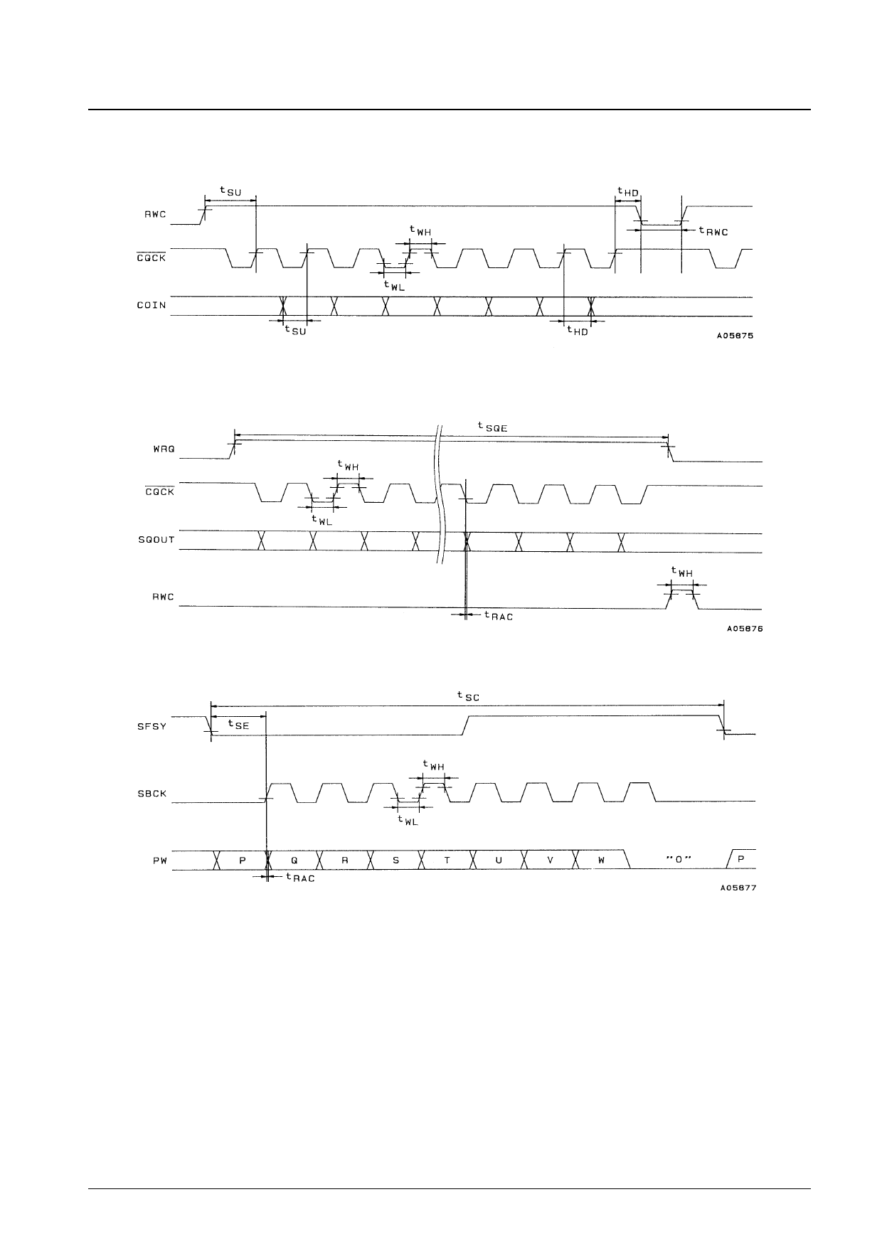
Figure 1 Command Input
Figure 2 Subcode Q Output
Figure 3 Subcode Output
No. 5480-5/29
5 Page 
LC78622E
• CLV mode
In CLV mode the LC78622E detects the disk speed from the HF signal and provides proper linear speed using
several different control schemes by switching the DSP internal modes. The PWM reference period corresponds to
a frequency of 7.35 kHz. The V/P pin outputs a high level during rough servo and a low level during phase control.
Internal mode
Rough servo (velocity too low)
Rough servo (velocity too high)
Phase control (PCK locked)
CLV+
High
Low
PWM
CLV–
Low
High
PWM
V/P
High
High
Low
• Rough servo gain switching
MSB
LSB
10101000
10101001
Command
DISC 8 SET
DISC 12 SET
RES = low
q
For 8 cm disks, the rough servo mode CLV control gain can be set about 8.5 dB lower than the gain used for 12 cm
disks.
• Phase control gain switching
MSB
LSB
10110001
10110010
10110011
10110000
Command
CLV PHASE COMPARATOR DIVISOR: 1/2
CLV PHASE COMPARATOR DIVISOR: 1/4
CLV PHASE COMPARATOR DIVISOR: 1/8
NO CLV PHASE COMPARATOR DIVISOR USED
RES= low
q
The phase control gain can be changed by changing the divisor used by the dividers in the stage immediately
preceding the phase comparator.
No. 5480-11/29
11 Page | ||
| Páginas | Total 29 Páginas | |
| PDF Descargar | [ Datasheet LC78622E.PDF ] | |
Hoja de datos destacado
| Número de pieza | Descripción | Fabricantes |
| LC78622E | Compact Disc Player DSP | Sanyo Semicon Device |
| LC78622NE | Compact Disc Player DSP | Sanyo Semicon Device |
| Número de pieza | Descripción | Fabricantes |
| SLA6805M | High Voltage 3 phase Motor Driver IC. |
Sanken |
| SDC1742 | 12- and 14-Bit Hybrid Synchro / Resolver-to-Digital Converters. |
Analog Devices |
|
DataSheet.es es una pagina web que funciona como un repositorio de manuales o hoja de datos de muchos de los productos más populares, |
| DataSheet.es | 2020 | Privacy Policy | Contacto | Buscar |
