|
|
|
PDF LC78631 Data sheet ( Hoja de datos )
| Número de pieza | LC78631 | |
| Descripción | Compact Disk Player DSP | |
| Fabricantes | Sanyo Semicon Device | |
| Logotipo | ||
Hay una vista previa y un enlace de descarga de LC78631 (archivo pdf) en la parte inferior de esta página. Total 30 Páginas | ||
|
No Preview Available !
Ordering number : EN 5342
CMOS LSI
LC78631E
Compact Disk Player DSP
Overview
The LC78631E is a compact disc D/A signal-processing
LSI for CD-ROM drives that provides a variable clock
error correction (VCEC) mode. The LC78631E
demodulates the EFM signal from the optical pickup and
performs de-interleaving, error detection, error correction,
digital filtering, and other processing. The LC78631E
includes an on-chip 1-bit D/A converter, and executes
commands sent from a control microprocessor.
Features
• VCEC support
• Built-in PLL circuit for EFM detection (supports 4×
playback)
• Built-in PLL for variable pitch playback (±13%)
• 18KB RAM on chip
• Error detection and correction (corrects two errors in C1
and four errors in C2)
• Frame jitter margin: ±8 frames
• Frame synchronization signal detection, protection, and
insertion
• Dual interpolation adopted in the interpolation circuit.
• EFM data demodulation
• Subcode demodulation
• Zero-cross muting adopted
• Servo command interface
• 2fs digital filter
• Digital de-emphasis
• Built-in independent left- and right-channel digital
attenuators (239 attenuation steps)
• Supports the bilingual function
• Left/right swap function
• Built-in 1-bit D/A converter (third-order ∆∑ noise
shaper, PWM output)
• Built-in digital output circuit
• CLV servo
• Arbitrary track jumping (of up to 255 tracks)
• Variable sled voltage (four levels)
• Six extended I/O ports and 2 extended output ports
• Built-in oscillator circuit using an external 16.9344 MHz
or 33.8688 MHz (for 4× playback) element
• Supply voltage: 3.6 to 5.5 V (4.75 to 5.5 V for 4×
playback mode)
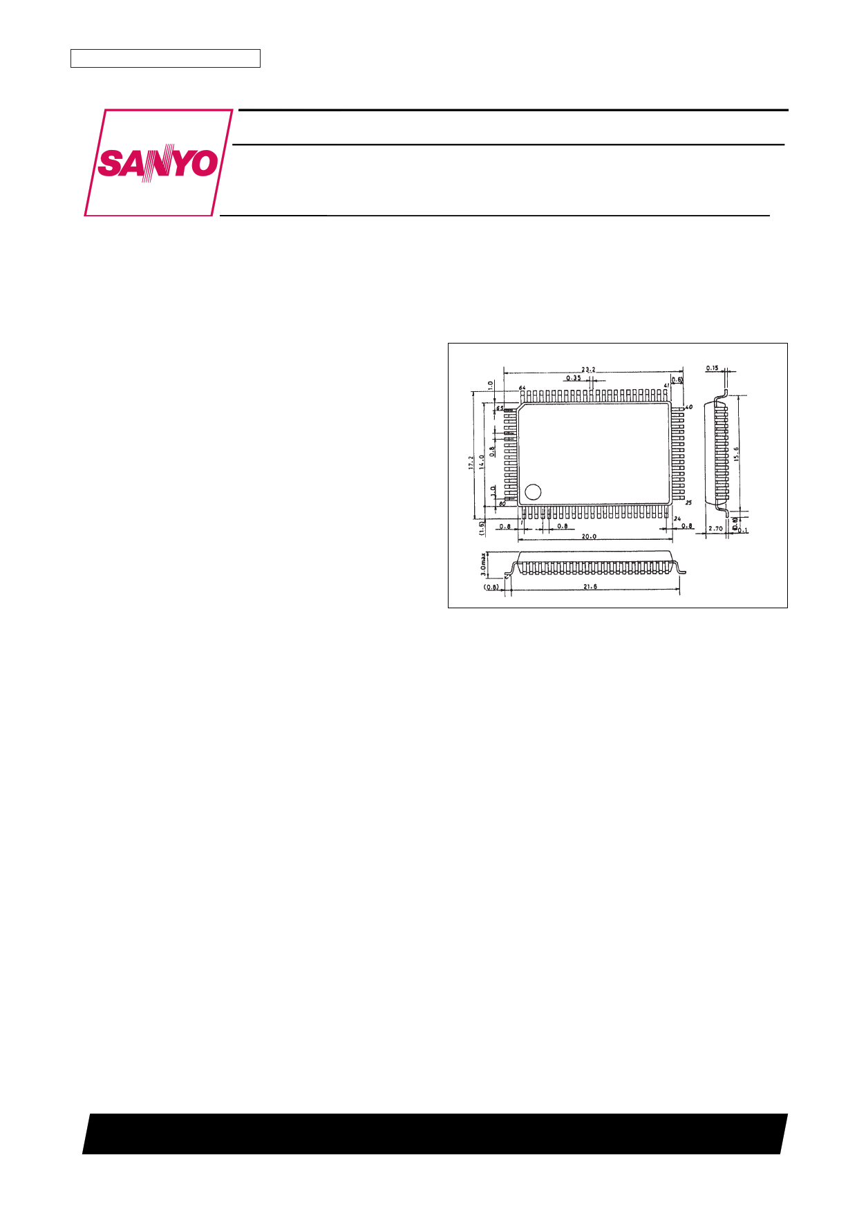
Package Dimensions
unit: mm
3174-QFP80E
[LC78631E]
SANYO: QFP80E
SANYO Electric Co.,Ltd. Semiconductor Bussiness Headquarters
TOKYO OFFICE Tokyo Bldg., 1-10, 1 Chome, Ueno, Taito-ku, TOKYO, 110 JAPAN
62096HA (OT) No. 5342-1/34
1 page 
LC78631E
D/A Converter Analog Characteristics at Ta = 25°C, VDD = 5 V, VSS = 0 V
Parameter
Total harmonic distortion
Dynamic range
Signal-to-noise ratio
Crosstalk
Symbol
THD + N
DR
S/N
CT
Conditions
LCHP, LCHN, RCHP, RCHN; 1 kHz: 0 dB input,
using a 20-kHz low-pass filter (AD725D built in)
LCHP, LCHN, RCHP, RCHN; 1 kHz: –60 dB input, using
the 20-kHz low-pass filter (A filter (AD725D built in))
LCHP, LCHN, RCHP, RCHN; 1 kHz: 0 dB input, using
the 20-kHz low-pass filter (A filter (AD725D built in))
LCHP, LCHN, RCHP, RCHN; 1 kHz: 0 dB input,
using a 20-kHz low-pass filter (AD725D built in)
min
98
96
typ
0.006
90
100
98
max
Unit
%
dB
dB
dB
Note: Measured in normal-speed playback mode in a Sanyo 1-bit D/A converter block reference circuit, with the digital attenuator set to EE (hexadecimal).
Figure 1 Command Input
Figure 2 Subcode Q Output
Figure 3 Subcode Output
No. 5342-5/34
5 Page 
LC78631E
4. Command input
An external controller can execute LC78631E instructions by setting RWC high and inputting commands to COIN in
synchronization with the CQCK clock. Commands are executed on the fall of the RWC signal.
• Single-byte commands
• Two-byte commands
• Command noise reduction
Code
$EF
$EE
Command
COMMAND INPUT NOISE REDUCTION MODE
CLEAR THE ABOVE MODE
RES = low
q
This command can reduce the noise on the CQCK clock signal. While this is effective for noise pulses under
500 ns, the use of this function requires that the CQCK timings tWL, tWH, and tSU (see Figure 1 and 2) be set to
1 µs or longer.
5. CLV servo circuit
• CLV servo circuit; Pin 13: CLV+, pin 14: CLV–, pin 15: V/P
Code
$04
$05
$06
$07
Command
DISC MOTOR START (accelerate)
DISC MOTOR CLV (CLV)
DISC MOTOR BRAKE (decelerate)
DISC MOTOR STOP (stop)
RES = low
q
The CLV+ signal causes the disc to accelerate in the forward direction, and CLV– causes the disc to decelerate. The
microcontroller can select one of four modes: accelerate, decelerate, CLV, and stop. The table below lists the states
of the CLV+ and CLV– pins in each of these modes.
Mode
Accelerate
Decelerate
CLV
Stop
CLV+
High
Low
Pulse output
Low
CLV–
Low
High
Pulse output
Low
Note: The CLV servo control commands only set the TOFF pin low during CLV mode. That pin will be at the high
level at all other times. Thus controlling the TOFF pin with microcontroller commands is only possible in
CLV mode.
No. 5342-11/34
11 Page | ||
| Páginas | Total 30 Páginas | |
| PDF Descargar | [ Datasheet LC78631.PDF ] | |
Hoja de datos destacado
| Número de pieza | Descripción | Fabricantes |
| LC78630 | Compact Disk Player DSP | Sanyo Semicon Device |
| LC78630E | Compact Disk Player DSP | Sanyo Semicon Device |
| LC78631 | Compact Disk Player DSP | Sanyo Semicon Device |
| LC78631E | Compact Disk Player DSP | Sanyo Semicon Device |
| Número de pieza | Descripción | Fabricantes |
| SLA6805M | High Voltage 3 phase Motor Driver IC. |
Sanken |
| SDC1742 | 12- and 14-Bit Hybrid Synchro / Resolver-to-Digital Converters. |
Analog Devices |
|
DataSheet.es es una pagina web que funciona como un repositorio de manuales o hoja de datos de muchos de los productos más populares, |
| DataSheet.es | 2020 | Privacy Policy | Contacto | Buscar |