|
|
|
PDF AWT6166R Data sheet ( Hoja de datos )
| Número de pieza | AWT6166R | |
| Descripción | GSM850/GSM900/DCS/PCS Quad Band Power Amplifier Module | |
| Fabricantes | ANADIGICS | |
| Logotipo | ||
Hay una vista previa y un enlace de descarga de AWT6166R (archivo pdf) en la parte inferior de esta página. Total 12 Páginas | ||
|
No Preview Available !
FEATURES
• Integrated Vreg (regulated supply)
• Harmonic Performance ≤ -20 dBm
• High Efficiency (PAE) at Pmax:
-GSM850, 53%
-GSM900, 55%
-DCS, 53%
-PCS, 53%
• +35 dBm GSM850/900 Output Power at 3.5 V
• +33 dBm DCS/PCS Output Power at 3.5 V
• 55 dB Dynamic Range
• GPRS Class 12 Capable
• RoHS Compliant Package, 250°C MSL-3
AWT6166R
GSM850/GSM900/DCS/PCS
Quad Band Powwwewr.DAatmaSphleifeite4rU.Mcoomdule
With Integrated Power Control
Data Sheet - Rev 2.0
APPLICATIONS
• Dual/Tri/Quad Band Handsets & PDAs
M15 Package
18 Pin 6 mm x 6 mm x 1.3 mm
Amplifier Module
PRODUCT DESCRIPTION
As with previous generations, the AWT6166R
integrated CMOS power control scheme simplifies
the design of the transmitter by eliminating the need
for external power control circuitry.
The AWT6166R input and output terminals are
internal matched to 50 ohms and DC blocked,
reducing the number of external components
required in the final application. Both PA die,
GSM850/900 and DCS/PCS, are fabricated using
state of the art InGaP HBT technology, known for it is
proven reliability and temperature stability.
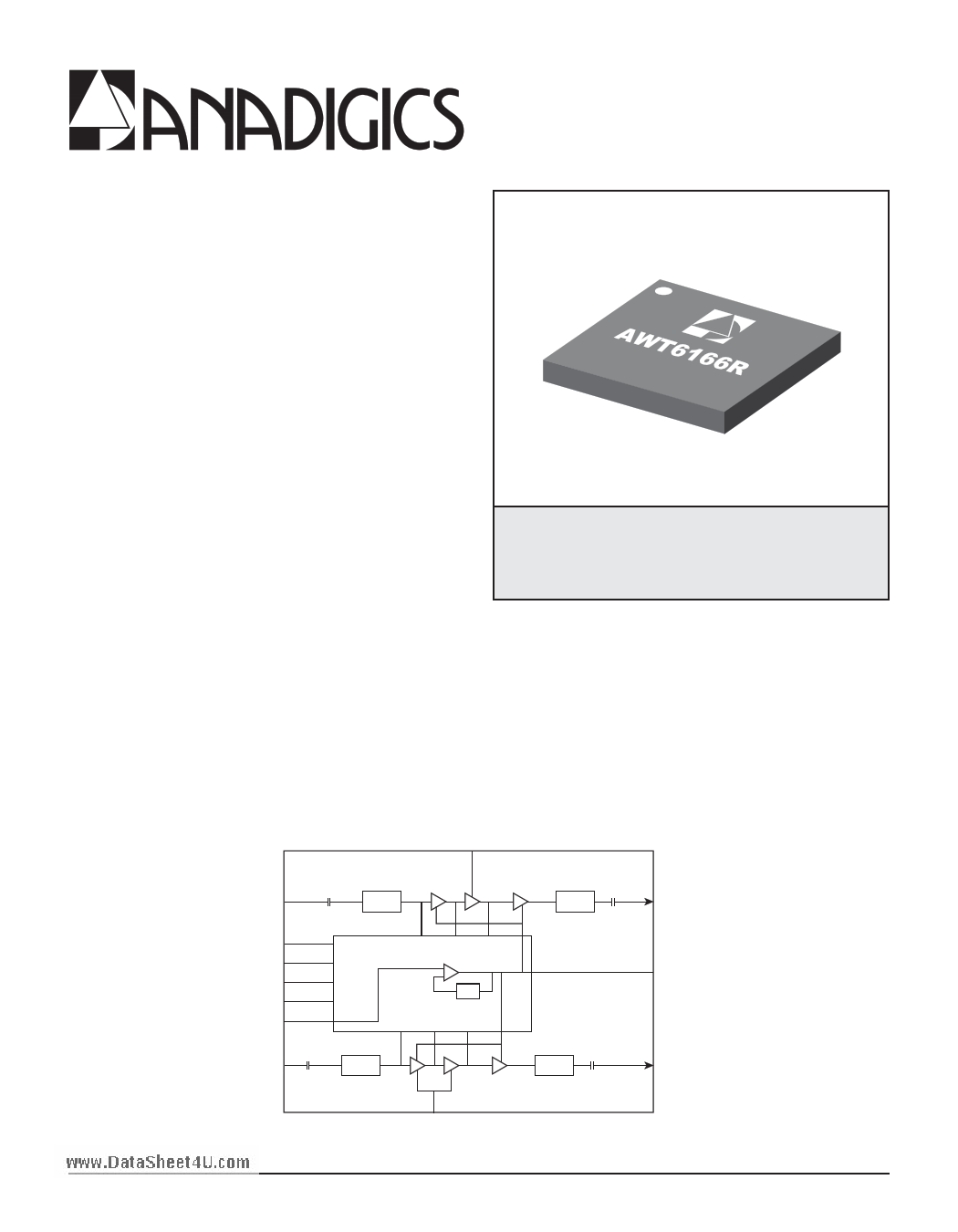
VCC2
DCS/PCSIN
BS
TX EN
VBATT
CEXT
VRAMP
GSM850/900IN
MATCH
CMOS BIAS/Integrated Power Control
H(s)
MATCH
MATCH
MATCH
VCC2
Figure 1: Block Diagram
02/2006
DCS/PCSOUT
VCC_OUT
GSM850/900OUT
1 page 
AWT6166R
PARAMETER
Table 5: Operating Ranges
MIN TYP MAX UNIT
www.DataSheet4U.com
COMMENTS
Case Temperature (TC)
-20 - 85 °C
Supply Voltage (VBATT)
3.0 3.5 4.8
V
Power Supply Leakage Current
VBATT = 4.8 V,
-
1
10
µA
VRAMP = 0 V,
TX_EN = LOW,
No RF applied
Control Voltage Range
0.2 - 1.6 V
Turn on time (TON)
Turn off time (TOFF)
Rise Time (TRISE)
Fall Time (TFALL)
VRAMP = 0.2 V, TX_EN =
- - 1 µs LOW → High
PIN = 5 dBm
VRAMP = 0.2 V, TX_EN =
- - 1 µs HIGH → LOW
PIN = 5 dBm
-
-
1
µs
POUT = -10 dBm →PMAX
(within 0.2 dB)
-
-
1
µs
POUT = PMAX→ -10 dBm
(within 0.2 dB)
VRAMP Input Capacitance
- 3 - pF
VRAMP Input Current
- - 10 µA
Duty Cycle
- - 50 %
The device may be operated safely over these conditions; however, parametric performance is
guaranteed only over the conditions defined in the electrical specifications.
Data Sheet - Rev 2.0
02/2006
5
5 Page 
PACKAGE OUTLINE
AWT6166R
www.DataSheet4U.com
Figure 5: M15 Package Outline - 18 Pin 6 mm x 6 mm x 1.3 mm Amplifier Module
Figure 6: Branding Specification
Data Sheet - Rev 2.0
02/2006
11
11 Page | ||
| Páginas | Total 12 Páginas | |
| PDF Descargar | [ Datasheet AWT6166R.PDF ] | |
Hoja de datos destacado
| Número de pieza | Descripción | Fabricantes |
| AWT6166 | GSM850/GSM900/DCS/PCS Quad Band Power Amplifier Module | ANADIGICS |
| AWT6166R | GSM850/GSM900/DCS/PCS Quad Band Power Amplifier Module | ANADIGICS |
| Número de pieza | Descripción | Fabricantes |
| SLA6805M | High Voltage 3 phase Motor Driver IC. |
Sanken |
| SDC1742 | 12- and 14-Bit Hybrid Synchro / Resolver-to-Digital Converters. |
Analog Devices |
|
DataSheet.es es una pagina web que funciona como un repositorio de manuales o hoja de datos de muchos de los productos más populares, |
| DataSheet.es | 2020 | Privacy Policy | Contacto | Buscar |