|
|
|
PDF TS4984FC Data sheet ( Hoja de datos )
| Número de pieza | TS4984FC | |
| Descripción | 1.2W Stereo Audio Power Amplifier with Active Low Standby Mode | |
| Fabricantes | STMicroelectronics | |
| Logotipo | ||
Hay una vista previa y un enlace de descarga de TS4984FC (archivo pdf) en la parte inferior de esta página. Total 30 Páginas | ||
|
No Preview Available !
www.DataSheet4U.com
TS4984FC
1.2W Stereo Audio Power Amplifier with
Active Low Standby Mode
■ Operating from VCC = 2.2V to 5.5V
■ 1.2W output power per channel @ VCC = 5V,
THD+N = 1%, RL = 8Ω
■ 10nA standby current
■ 62dB PSRR @ 217Hz with grounded inputs
■ High SNR: 106dB(A) typ.
■ Near-zero pop & click
■ Available in a 15-bump flip-chip (lead-free)
Description
The TS4984 has been designed for top-class
stereo audio applications. Thanks to its compact
and power dissipation efficient flip-chip package, it
suits various applications.
With a output BTL configuration, this audio power
amplifier is capable of delivering 1.2W per
channel of continuous RMS output power into an
8Ω load @ 5V.
An externally-controlled standby mode reduces
the supply current to less than 10nA per channel.
The device also features an internal thermal
shutdown protection.
The gain of each channel can be configured by
external gain setting resistors.
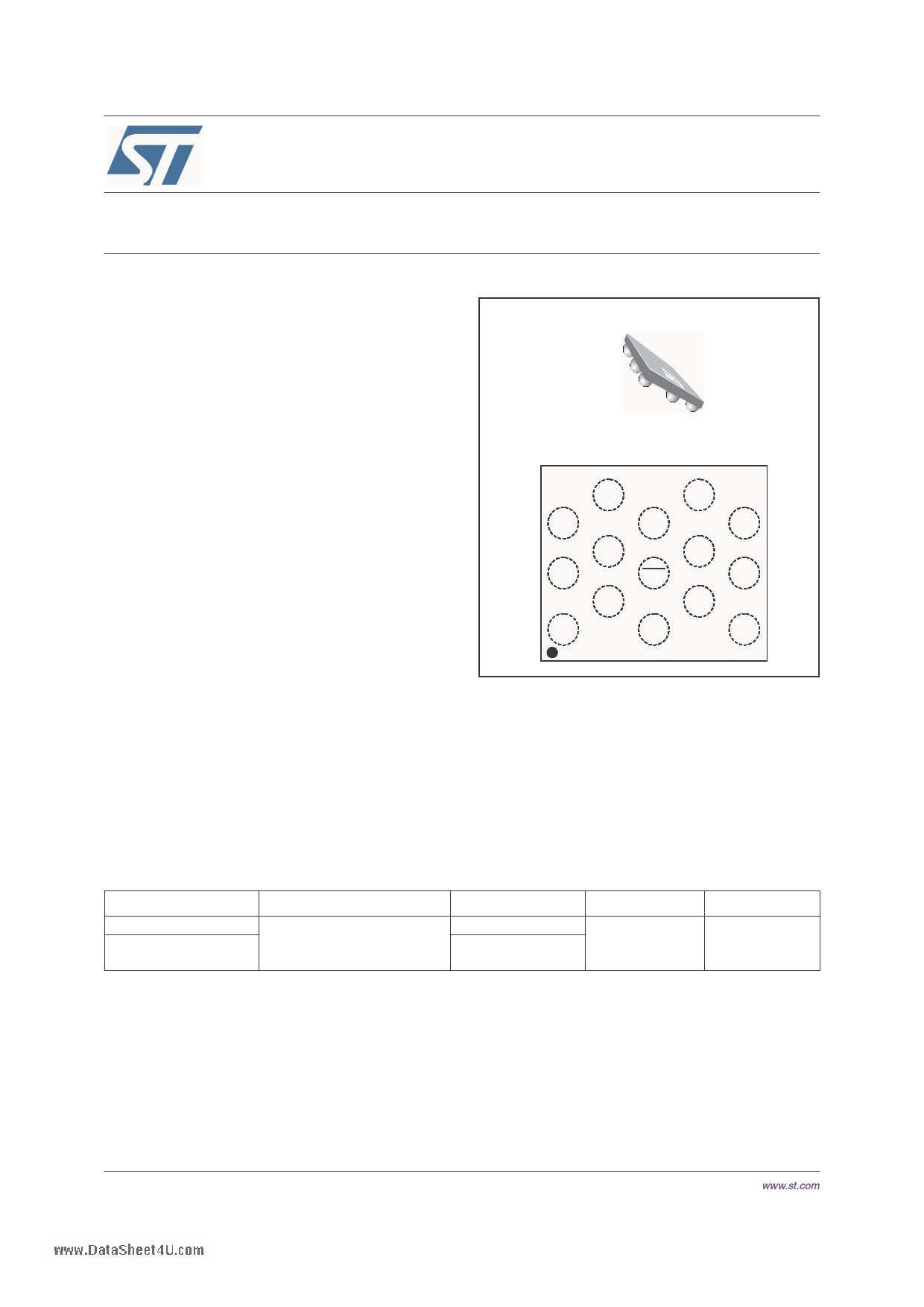
TS4984 - flip-chip 15 bumps
Pin connections (top view)
VCC
VCC
BYPASS
IN2+
IN2-
VOUT1-
VOUT1+
STDBY
VOUT2+
VOUT2-
IN1+
GND
IN1-
BYPASS
GND
Applications
■ Cellular mobile phones
■ Notebook & PDA computers
■ LCD monitors & TVs
■ Portable audio devices
Order Codes
Part Number
TS4984EIJT
TS4984EIKJT
Temperature Range
-40, +85°C
Package
Lead free flip-chip
Lead free flip-chip +
back coating
Packing
Tape & Reel
Marking
A84
November 2005
Rev 2
1/30
www.st.com
30
1 page 
TS4984FC
ElectricalwCwhwa.DraatcatSehreiestt4iUc.csom
Table 5.
Symbol
VCC = +3.3V, GND = 0V, Tamb = 25°C (unless otherwise specified)
Parameter
Min. Typ.
Max.
Unit
ICC Supply Current
No input signal, no load
6.6 12
mA
ISTBY Standby Current (1)
No input signal, VSTBY = GND, RL = 8Ω
10 1000 nA
VOO Output Offset Voltage
No input signal, RL = 8Ω
1 10 mV
Pout Output Power
THD = 1% Max, F = 1kHz, RL = 8Ω
375 500
mW
THD + N
Total Harmonic Distortion
+ Noise
Pout = 400mWrms, AV = 2
20Hz ≤ F ≤ 20kHz, RL = 8Ω
0.1 %
Power Supply Rejection
PSRR Ratio(2)
RL = 8Ω, AV = 2, Vripple = 200mVpp,
Input Grounded, F = 217Hz
RL = 8Ω, AV = 2, Vripple = 200mVpp,
Input Grounded, F = 1kHz
55 61
55 63
dB
Crosstalk Channel Separation,
RL = 8Ω, F = 1kHz
RL = 8Ω, F = 20Hz to 20kHz
107
dB
82
twu Wake-Up Time
Cb = 1µF
110 140
ms
tstby Standby Time
Cb = 1µF
10 µs
VSTBYH
Standby Voltage Level
High
1.2 V
VSTBYL
Standby Voltage Level
Low
0.4 V
ΦM
Phase Margin at Unity
Gain
RL = 8Ω, CL = 500pF
65 Degrees
GM Gain Margin
RL = 8Ω, CL = 500pF
15 dB
GBP Gain Bandwidth Product RL = 8Ω
1.5 MHz
1. Standby mode is activated when VSTBY is tied to Gnd.
2. All PSRR data limits are guaranteed by production sampling tests.
Dynamic measurements - 20*log(rms(Vout)/rms(Vripple)). Vripple is the sinusoidal signal superimposed upon VCC.
5/30
5 Page 
TS4984FC
ElectricalwCwhwa.DraatcatSehreiestt4iUc.csom
Figure 20. Power supply rejection ratio (PSRR) Figure 21. Power supply rejection ratio (PSRR)
vs. DC output voltage
vs. DC output voltage
0
Vcc = 2.6V
-10 Vripple = 200mVpp
RL = 8Ω
-20 Cb = 1µF
AV = 2
Tamb = 25°C
-30
-40
-50
-60
-70
-2.5 -2.0 -1.5 -1.0 -0.5 0.0 0.5 1.0 1.5 2.0 2.5
Differential DC Output Voltage (V)
0
Vcc = 2.6V
-10
Vripple = 200mVpp
RL = 8Ω
Cb = 1µF
-20 AV = 5
Tamb = 25°C
-30
-40
-50
-60
-2.5 -2.0 -1.5 -1.0 -0.5 0.0 0.5 1.0 1.5 2.0 2.5
Differential DC Output Voltage (V)
Figure 22. Power supply rejection ratio (PSRR) Figure 23. Power supply rejection ratio (PSRR)
vs. DC output voltage
at F = 217Hz vs. bypass capacitor
0
Vcc = 2.6V
Vripple = 200mVpp
-10 RL = 8Ω
Cb = 1µF
AV = 10
-20 Tamb = 25°C
-30
-40
-50
-2.5 -2.0 -1.5 -1.0 -0.5 0.0 0.5 1.0 1.5 2.0 2.5
Differential DC Output Voltage (V)
-30
-40
-50
Av=2
-60 Vcc:
2.6V
3.3V
-70 5V
-80
0.1
Av=10
Vcc:
2.6V
3.3V
5V
Av=5
Vcc:
2.6V
3.3V
5V
Tamb=25°C
1
Bypass Capacitor Cb ( F)
Figure 24. Output power vs. power supply
voltage
Figure 25. Output power vs. power supply
voltage
11/30
11 Page | ||
| Páginas | Total 30 Páginas | |
| PDF Descargar | [ Datasheet TS4984FC.PDF ] | |
Hoja de datos destacado
| Número de pieza | Descripción | Fabricantes |
| TS4984FC | 1.2W Stereo Audio Power Amplifier with Active Low Standby Mode | STMicroelectronics |
| Número de pieza | Descripción | Fabricantes |
| SLA6805M | High Voltage 3 phase Motor Driver IC. |
Sanken |
| SDC1742 | 12- and 14-Bit Hybrid Synchro / Resolver-to-Digital Converters. |
Analog Devices |
|
DataSheet.es es una pagina web que funciona como un repositorio de manuales o hoja de datos de muchos de los productos más populares, |
| DataSheet.es | 2020 | Privacy Policy | Contacto | Buscar |