|
|
|
PDF NB4N11S Data sheet ( Hoja de datos )
| Número de pieza | NB4N11S | |
| Descripción | 3.3V 1:2 AnyLevel Input to LVDS Fanout Buffer /Translator | |
| Fabricantes | ON Semiconductor | |
| Logotipo | ||
Hay una vista previa y un enlace de descarga de NB4N11S (archivo pdf) en la parte inferior de esta página. Total 10 Páginas | ||
|
No Preview Available !
NB4N11S
3.3 V 1:2 AnyLevel™ Input
to LVDS Fanout Buffer /
Translator
The NB4N11S is a differential 1:2 Clock or Data Receiver and will
accept AnyLevelTM input signals: LVPECL, CML, LVCMOS,
LVTTL, or LVDS. These signals will be translated to LVDS and two
identical copies of Clock or Data will be distributed, operating up to
2.0 GHz or 2.5 Gb/s, respectively. As such, the NB4N11S is ideal for
SONET, GigE, Fiber Channel, Backplane and other Clock or Data
distribution applications.
The NB4N11S has a wide input common mode range from
GND + 50 mV to VCC − 50 mV. Combined with the 50 W internal
termination resistors at the inputs, the NB4N11S is ideal for
translating a variety of differential or single−ended Clock or Data
signals to 350 mV typical LVDS output levels.
The NB4N11S is functionally equivalent to the EP11, LVEP11,
SG11 or 7L11M devices and is offered in a small 3 mm X 3 mm
16−QFN package. Application notes, models, and support
documentation are available at www.onsemi.com.
Features
• Maximum Input Clock Frequency > 2.0 GHz
• Maximum Input Data Rate > 2.5 Gb/s
• 1 ps Maximum of RMS Clock Jitter
• Typically 10 ps of Data Dependent Jitter
• 380 ps Typical Propagation Delay
• 120 ps Typical Rise and Fall Times
• Functionally Compatible with Existing 3.3 V LVEL, LVEP, EP, and
SG Devices
Device DDJ = 10 ps
www.DataSheet4U.com
http://onsemi.com
1
QFN−16
MN SUFFIX
CASE 485G
MARKING
DIAGRAM*
16
1
NB4N
11S
ALYW
A = Assembly Location
L = Wafer Lot
Y = Year
W = Work Week
*For additional marking information, refer to
Application Note AND8002/D.
Q0
VTD Q0
D
D
VTD
Figure 1. Logic Diagram
Q1
Q1
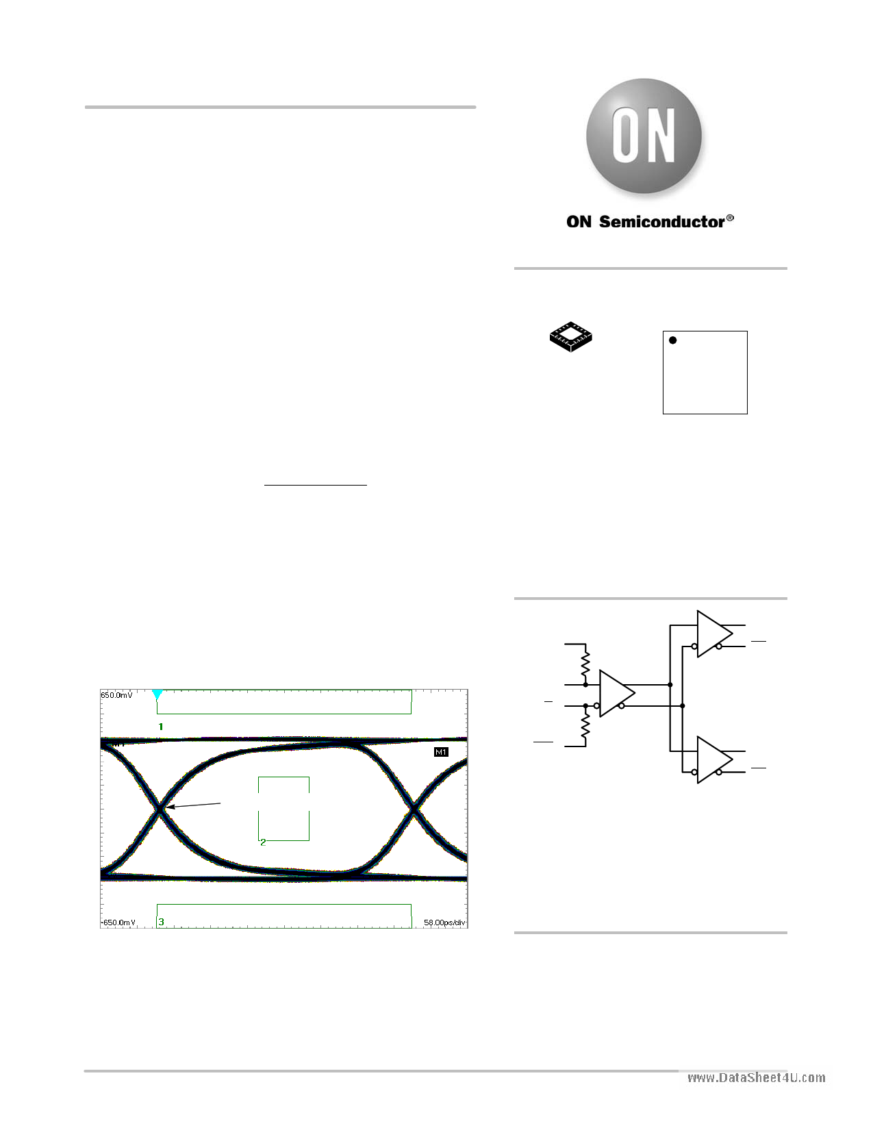
TIME (58 ps/div)
Figure 2. Typical Output Waveform at 2.488 Gb/s with
PRBS 223−1 (VINPP = 400 mV; Input Signal DDJ = 14 ps)
ORDERING INFORMATION
See detailed ordering and shipping information in the package
dimensions section on page 9 of this data sheet.
© Semiconductor Components Industries, LLC, 2005
December, 2005 − Rev. 0
1
Publication Order Number:
NB4N11S/D
1 page 
NB4N11S
Table 5. AC CHARACTERISTICS VCC = 3.0 V to 3.6 V, GND = 0 V; (Note 10)
−40°C
25°C
85°wC ww.DataSheet4U.com
Symbol
Characteristic
Min Typ Max Min Typ Max Min Typ Max Unit
VOUTPP
Output Voltage Amplitude (@ VINPPmin) fin ≤ 1.0 GHz
(Figure 4)
fin= 1.5 GHz
fin= 2.0 GHz
220
200
170
350
300
270
250 350
200 300
170 270
250 350
200 300
170 270
mV
fDATA Maximum Operating Data Rate
1.5 2.5
1.5 2.5
1.5 2.5
Gb/s
tPLH,
tPHL
Differential Input to Differential Output
Propagation Delay
270 370 470 270 370 470 270 370 470 ps
tSKEW
Duty Cycle Skew (Note 11)
Within Device Skew (Note 16)
Device−to−Device Skew (Note 15)
8 45
5 25
30 100
8 45
5 25
30 100
8 45 ps
5 25
30 100
tJITTER
VINPP
RMS Random Clock Jitter (Note 13) fin = 1.0 GHz
fin = 1.5 GHz
Deterministic Jitter (Note 14) fDATA = 622 Mb/s
fDATA = 1.5 Gb/s
fDATA = 2.488 Gb/s
Input Voltage Swing/Sensitivity
(Differential Configuration) (Note 12)
100
0.5 1
0.5 1
6
7 20
10 20
VCC− 100
GND
0.5 1
0.5 1
6
7 20
10 20
VCC− 100
GND
0.5 1
0.5 1
6
7 20
10 20
ps
VCC− mV
GND
tr Output Rise/Fall Times @ 250 MHz
tf (20% − 80%)
Q, Q 70 120 170 70 120 170 70 120 170 ps
NOTE: Device will meet the specifications after thermal equilibrium has been established when mounted in a test socket or printed circuit
board with maintained transverse airflow greater than 500 lfpm. Electrical parameters are guaranteed only over the declared
operating temperature range. Functional operation of the device exceeding these conditions is not implied. Device specification limit
values are applied individually under normal operating conditions and not valid simultaneously.
10. Measured by forcing VINPPmin with 50% duty cycle clock source and VCC − 1400 mV offset. All loading with an external RL = 100 W across
“D” and “D” of the receiver. Input edge rates 150 ps (20%−80%).
11. See Figure 13 differential measurement of tskew = |tPLH − tPHL| for a nominal 50% differential clock input waveform @ 250 MHz.
12. Input voltage swing is a single−ended measurement operating in differential mode.
13. RMS jitter with 50% Duty Cycle clock signal at 750 MHz.
14. Deterministic jitter with input NRZ data at PRBS 223−1 and K28.5.
15. Skew is measured between outputs under identical transition @ 250 MHz.
16. The worst case condition between Q0/Q0 and Q1/Q1 from either D0/D0 or D1/D1, when both outputs have the same transition.
400
350
300
−40°C
250
200 85°C
25°C
150
100
50
0
0 0.5 1 1.5 2 2.5 3
INPUT CLOCK FREQUENCY (GHz)
Figure 4. Output Voltage Amplitude (VOUTPP) versus
Input Clock Frequency (fin) and Temperature (@ VCC = 3.3 V)
http://onsemi.com
5
5 Page | ||
| Páginas | Total 10 Páginas | |
| PDF Descargar | [ Datasheet NB4N11S.PDF ] | |
Hoja de datos destacado
| Número de pieza | Descripción | Fabricantes |
| NB4N111K | 3.3V Differential In 1:10 Differential Fanout Clock Driver | ON Semiconductor |
| NB4N1158 | Link Replicator | ON Semiconductor |
| NB4N11M | Multi Level Clock/Data Input to CML Receiver/ Buffer/ Translator | ON Semiconductor |
| NB4N11S | 3.3V 1:2 AnyLevel Input to LVDS Fanout Buffer /Translator | ON Semiconductor |
| Número de pieza | Descripción | Fabricantes |
| SLA6805M | High Voltage 3 phase Motor Driver IC. |
Sanken |
| SDC1742 | 12- and 14-Bit Hybrid Synchro / Resolver-to-Digital Converters. |
Analog Devices |
|
DataSheet.es es una pagina web que funciona como un repositorio de manuales o hoja de datos de muchos de los productos más populares, |
| DataSheet.es | 2020 | Privacy Policy | Contacto | Buscar |