|
|
PDF SSTU32864 Data sheet ( Hoja de datos )
| Número de pieza | SSTU32864 | |
| Descripción | 1.8V confgurable registered buffer | |
| Fabricantes | NXP Semiconductors | |
| Logotipo | ||
Hay una vista previa y un enlace de descarga de SSTU32864 (archivo pdf) en la parte inferior de esta página. Total 19 Páginas | ||
|
No Preview Available !
SSTU32864
1.8 V configurable registered buffer
for DDR2 RDIMM applications
Rev. 01 — 12 July 2004
www.DataSheet4U.com
Objective data
1. Description
The SSTU32864 is a 25-bit 1:1 or 14-bit 1:2 configurable registered buffer designed
for 1.7 V to 1.9 V VDD operation.
All clock and data inputs are compatible with the JEDEC standard to SSTL_18. The
control inputs are LVCMOS. All outputs are 1.8 V CMOS drivers that have been
optimized to drive the DDR2 DIMM load.
The SSTU32864 operates from a differential clock (CK and CK). Data are registered
at the crossing of CK going HIGH, and CK going LOW.
The C0 input controls the pinout configuration of the 1:2 pinout from A configuration
(when LOW) to B configuration (when HIGH). The C1 input controls the pinout
configuration from 25-bit 1:1 (when LOW) to 14-bit 1:2 (when HIGH).
The device supports low-power standby operation. When the reset input (RESET) is
LOW, the differential input receivers are disabled, and undriven (floating) data, clock
and reference voltage (VREF) inputs are allowed. In addition, when RESET is LOW all
registers are reset, and all outputs are forced LOW. The LVCMOS RESET and Cn
inputs must always be held at a valid logic HIGH or LOW level.
To ensure defined outputs from the register before a stable clock has been supplied,
RESET must be held in the LOW state during power-up.
In the DDR2 RDIMM application, RESET is specified to be completely asynchronous
with respect to CK and CK. Therefore, no timing relationship can be guaranteed
between the two. When entering reset, the register will be cleared and the data
outputs will be driven LOW quickly, relative to the time to disable the differential input
receivers. However, when coming out of reset, the register will become active quickly,
relative to the time to enable the differential input receivers. As long as the data inputs
are LOW, and the clock is stable during the time from the LOW-to-HIGH transition of
RESET until the input receivers are fully enabled, the design of the SSTU32864 must
ensure that the outputs will remain LOW, thus ensuring no glitches on the output.
The device monitors both DCS and CSR inputs and will gate the Qn outputs from
changing states when both DCS and CSR inputs are HIGH. If either DCS or CSR
input is LOW, the Qn outputs will function normally. The RESET input has priority over
the DCS and CSR control and will force the outputs LOW. If the DCS-control
functionality is not desired, then the CSR input can be hardwired to ground, in which
case the setup time requirement for DCS would be the same as for the other D data
inputs.
The SSTU32864 is available in the LFBGA96 package.
1 page 
Philips Semiconductors
SSTU32864
1.8 V configurable registered buffer for DDR2 RDIMM applications
www.DataSheet4U.com
4.2 Pin description
Table 2: Pin description
Symbol Description
Electrical
characteristics
GND
Ground
ground input
VDD
VREF
ZOH
ZOL
CK
Power supply voltage
Input reference voltage
Reserved for future use
Reserved for future use
Positive master clock input
1.8 V nominal
0.9 V nominal
input
input
differential input
CK Negative master clock input
differential input
C0, C1
Configuration control inputs
LVCMOS inputs
RESET
CSR, DCS
Asynchronous reset input. Resets registers and disables
VREF data and clock differential-input receivers.
Chip select inputs. Disables data outputs switching when
both inputs are HIGH (see Table note [1]).
LVCMOS input
SSTL_18 input
D[1:25]
Data inputs. Clocked in on the crossing of the rising edge of SSTL_18 input
CK and the falling edge of CK.
DODT
The outputs of this register will not be suspended by DCS
and CSR control.
SSTL_18 input
DCKE
The outputs of this register will not be suspended by DCS
and CSR control.
SSTL_18 input
Q[1:25]
The outputs that are suspended by DCS and CSR control
(see Table note [2]).
1.8 V CMOS
QCS
Data outputs that will not be suspended by DCS and CSR
control.
1.8 V CMOS
QODT
Data outputs that will not be suspended by DCS and CSR
control.
1.8 V CMOS
QCKE
Data outputs that will not be suspended by DCS and CSR
control.
1.8 V CMOS
n.c. No-connect. Ball present but no internal connection to the -
die.
DNU
Do-not-use. Ball internally connected to the die which should -
be left open-circuit.
[1] Configurations:
Data inputs = D2, D3, D5, D6, D8-D25 when C0 = 0 and C1 = 0.
Data inputs = D2, D3, D5, D6, D8-D14 when C0 = 0 and C1 = 1.
Data inputs = D1-D6, D8-D10, D12, D13 when C0 = 1 and C1 = 1.
[2] Configurations:
Data outputs = Q2, Q3, Q5, Q6, Q8-Q25 when C0 = 0 and C1 = 0.
Data outputs = Q2, Q3, Q5, Q6, Q8-Q14 when C0 = 0 and C1 = 1.
Data outputs = Q1-Q6, Q8-Q10, Q12, Q13 when C0 = 1 and C1 = 1.
9397 750 13339
Objective data
Rev. 01 — 12 July 2004
© Koninklijke Philips Electronics N.V. 2004. All rights reserved.
5 of 19
5 Page 
Philips Semiconductors
10. Test information
SSTU32864
1.8 V configurable registered buffer for DDR2 RDIMM applications
www.DataSheet4U.com
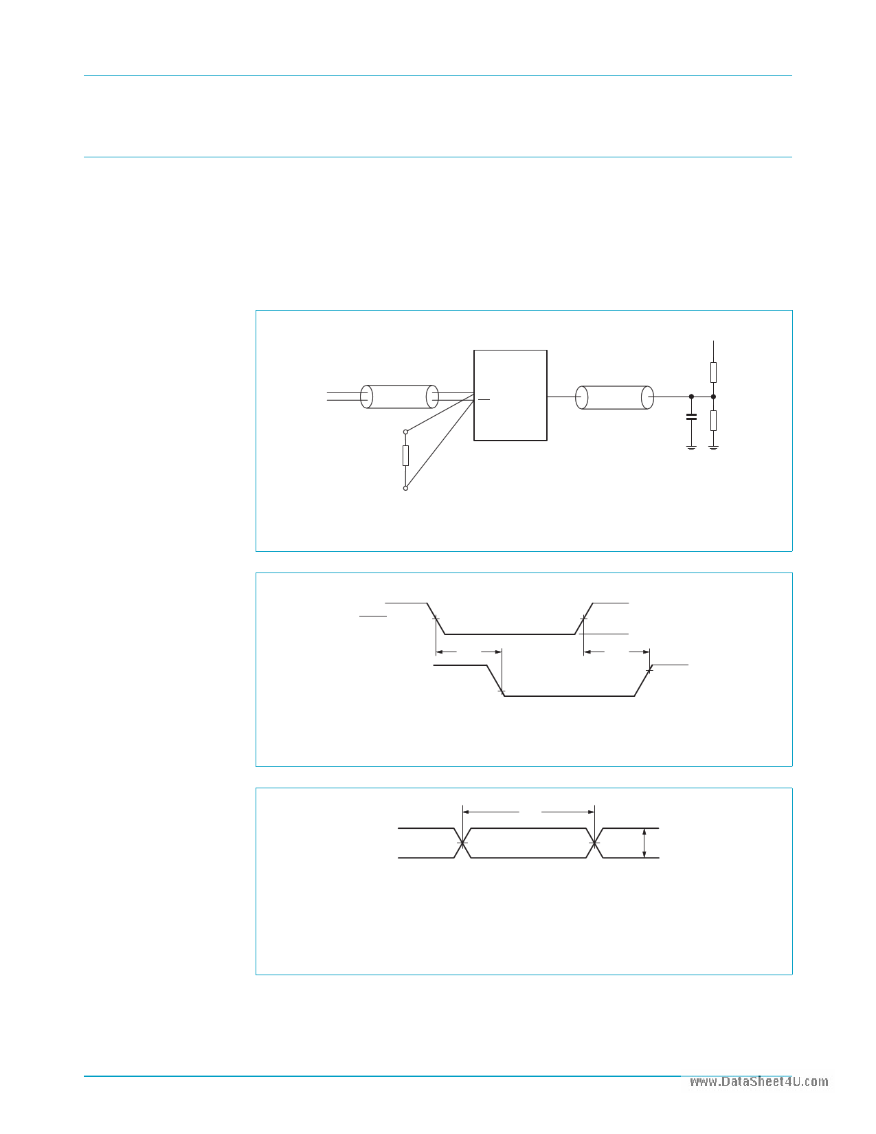
10.1 Test circuit
All input pulses are supplied by generators having the following characteristics:
PRR ≤ 10 MHz; Zo = 50 Ω; input slew rate = 1 V/ns ± 20%, unless otherwise
specified.
The outputs are measured one at a time with one transition per measurement.
CK INPUTS
TL = 50 Ω
TEST POINT
RL = 100 Ω
DUT
CK
CK
OUT
TEST POINT
(1) CL includes probe and jig capacitance.
Fig 5. Load circuit.
VDD
TL = 350 ps, 50 Ω
RL = 1000 Ω
CL = 30 pF
SEE NOTE (1)
RL = 1000 Ω
002aaa371
LVCMOS
RESET
VDD/2
IDD
(SEE NOTE)
tinact
10%
VDD/2
VDD
0V
tact
90%
002aaa372
IDD tested with clock and data inputs held at VDD or GND, and Io = 0 mA.
Fig 6. Voltage and current waveforms; inputs active and inactive times.
INPUT
VICR
tW
VICR
VIH
VID
VIL
002aaa373
VID = 600 mV
VIH = VREF + 250 mV (AC voltage levels) for differential inputs. VIH = VDD for LVCMOS inputs.
VIL = VREF − 250 mV (AC voltage levels) for differential inputs. VIL = GND for LVCMOS inputs.
Fig 7. Voltage waveforms; pulse duration.
9397 750 13339
Objective data
Rev. 01 — 12 July 2004
© Koninklijke Philips Electronics N.V. 2004. All rights reserved.
11 of 19
11 Page | ||
| Páginas | Total 19 Páginas | |
| PDF Descargar | [ Datasheet SSTU32864.PDF ] | |
Hoja de datos destacado
| Número de pieza | Descripción | Fabricantes |
| SSTU32864 | 1.8V confgurable registered buffer | NXP Semiconductors |
| SSTU32865 | 28-bit 1:2 registered buffer | NXP Semiconductors |
| SSTU32866 | 1.8V 25-bit 1:1 or 14-bit 1:2 confgurable registered buffer | NXP Semiconductors |
| Número de pieza | Descripción | Fabricantes |
| SLA6805M | High Voltage 3 phase Motor Driver IC. |
Sanken |
| SDC1742 | 12- and 14-Bit Hybrid Synchro / Resolver-to-Digital Converters. |
Analog Devices |
|
DataSheet.es es una pagina web que funciona como un repositorio de manuales o hoja de datos de muchos de los productos más populares, |
| DataSheet.es | 2020 | Privacy Policy | Contacto | Buscar |
