|
|
|
PDF ISLA118P50 Data sheet ( Hoja de datos )
| Número de pieza | ISLA118P50 | |
| Descripción | 500MSPS A/D Converter | |
| Fabricantes | Intersil | |
| Logotipo | ||
Hay una vista previa y un enlace de descarga de ISLA118P50 (archivo pdf) en la parte inferior de esta página. Total 30 Páginas | ||
|
No Preview Available !
www.DataSheet4U.com
8-Bit, 500MSPS A/D Converter
ISLA118P50
The ISLA118P50 is a low-power, high-performance,
500MSPS analog-to-digital converter designed with
Intersil’s proprietary FemtoCharge® technology on a
standard CMOS process. The ISLA118P50 is part of a
pin-compatible portfolio of 8, 10 and 12-bit A/Ds. This
device an upgrade of the KAD551XP-50 product family
and is pin similar.
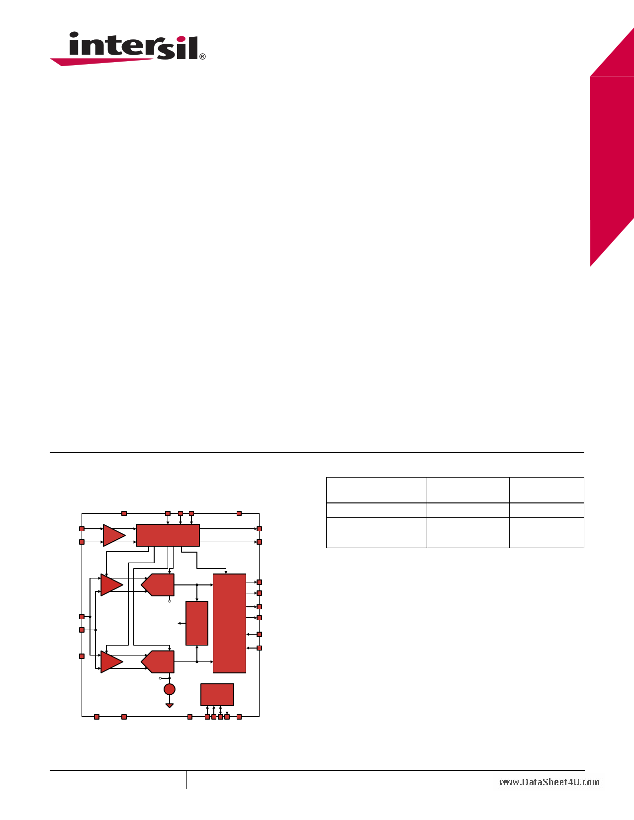
The device utilizes two time-interleaved 250MSPS unit
A/Ds to achieve the ultimate sample rate of 500MSPS. A
single 500MHz conversion clock is presented to the
converter, and all interleave clocking is managed
internally. The proprietary Intersil Interleave Engine
(I2E) performs automatic fine correction of offset, gain,
and sample time skew mismatches between the unit
A/Ds to optimize performance. No external interleaving
algorithm is required.
A serial peripheral interface (SPI) port allows for
extensive configurability of the A/D. The SPI also controls
the interleave correction circuitry, allowing the system to
issue continuous calibration commands as well as
configure many dynamic parameters.
Digital output data is presented in selectable LVDS or
CMOS formats. The ISLA118P50 is available in a
72-contact QFN package with an exposed paddle.
Performance is specified over the full industrial
temperature range (-40°C to +85°C).
Features
• 1.15GHz Analog Input Bandwidth
• 90fs Clock Jitter
• Automatic Fine Interleave Correction Calibration
• Multiple Chip Time Alignment Support via the
Synchronous Clock Divider Reset
• Programmable Gain, Offset and Skew control
• Over-Range Indicator
• Selectable Clock Divider: ÷1 or ÷2
• Clock Phase Selection
• Nap and Sleep Modes
• Two’s Complement, Gray Code or Binary Data
Format
• DDR LVDS-Compatible or LVCMOS Outputs
• Programmable Test Patterns and Internal
Temperature Sensor
Applications
• Radar and Electronic/Signal Intelligence
• Broadband Communications
• High-Performance Data Acquisition
Block Diagram
CLKP
CLKN
CLOCK
MANAGEMENT
CLKOUTP
CLKOUTN
VINP
VINN
VCM
SHA
SHA
8 -BIT
250 MSPS
ADC
VREF
Gain/ Offset/ Skew
Adjustments
DIGITAL
I2E ERROR
CORRECTION
8 -BIT
250 MSPS
ADC
VREF
1.25V
+
–
SPI
CONTROL
D[7:0]P
D[7:0]N
ORP
ORN
OUTFMT
OUTMODE
Pin-Compatible Family
MODEL
ISLA112P50
ISLA110P50
ISLA118P50
RESOLUTION
12
10
8
SPEED
(MSPS)
500
500
500
Key Specifications
• SNR = 49.9dBFS for fIN = 190MHz (-1dBFS)
• SFDR = 68dBc for fIN = 190MHz (-1dBFS)
• Total Power Consumption = 428mW
March 30, 2010
FN7565.0
1 CAUTION: These devices are sensitive to electrostatic discharge; follow proper IC Handling Procedures.
1-888-INTERSIL or 1-888-468-3774 | Intersil (and design) is a registered trademark of Intersil Americas Inc.
FemtoCharge is a trademark of Kenet Inc. Copyright Intersil Americas Inc. 2010. All Rights Reserved
All other trademarks mentioned are the property of their respective owners.
1 page 
ISLA118P50
www.DataSheet4U.com
Absolute Maximum Ratings
Thermal Information
AVDD to AVSS . . . . . . . . . . . . . . . . . . . . . . . -0.4V to 2.1V
OVDD to OVSS. . . . . . . . . . . . . . . . . . . . . . . -0.4V to 2.1V
AVSS to OVSS . . . . . . . . . . . . . . . . . . . . . . . -0.3V to 0.3V
Analog Inputs to AVSS . . . . . . . . . . . -0.4V to AVDD + 0.3V
Clock Inputs to AVSS . . . . . . . . . . . . -0.4V to AVDD + 0.3V
Logic Input to AVSS . . . . . . . . . . . . . -0.4V to OVDD + 0.3V
Logic Inputs to OVSS . . . . . . . . . . . . -0.4V to OVDD + 0.3V
Thermal Resistance (Typical)
θJA (°C/W) θJC (°C/W)
72 Ld QFN (Notes 3, 4, 5) . . . . . . . 23
0.75
Storage Temperature . . . . . . . . . . . . . . . . -65°C to +150°C
Junction Temperature . . . . . . . . . . . . . . . . . . . . . . +150°C
Pb-Free Reflow Profile . . . . . . . . . . . . . . . . . .see link below
http://www.intersil.com/pbfree/Pb-FreeReflow.asp
Recommended Operating Conditions
Operating Temperature . . . . . . . . . . . . . . . -40°C to +85°C
NOTES:
3. θJA is measured in free air with the component mounted on a high effective thermal conductivity test board with “direct attach”
features. See Tech Brief TB379 for details.
4. For θJC, the “case temp” location is the center of the exposed metal pad on the package underside.
5. For solder stencil layout and reflow guidelines, please see Tech Brief TB389.
CAUTION: Do not operate at or near the maximum ratings listed for extended periods of time. Exposure to such conditions may adversely impact
product reliability and result in failures not covered by warranty.
Electrical Specifications
All specifications apply under the following conditions unless otherwise noted: AVDD = 1.8V,
OVDD = 1.8V, TA = -40°C to +85°C (typical specifications at +25°C), AIN = -1dBFS,
FIN = 105MHz, fSAMPLE = 500MSPS, after completion of I2E calibration.
ISLA118P50
(Note 6)
PARAMETER
SYMBOL
CONDITIONS
MIN TYP MAX UNITS
DC SPECIFICATIONS (Note 6)
Analog Input
Full-Scale Analog Input Range
Input Resistance
Input Capacitance
Full Scale Range Temp. Drift
Input Offset Voltage
Gain Error
Common-Mode Output Voltage
Clock Inputs
VFS
RIN
CIN
AVTC
VOS
EG
VCM
Differential
Differential
Differential
Full Temp
1.41
-10
435
1.45
500
1.9
325
±2.0
±2.0
535
1.52
10
635
VP-P
Ω
pF
ppm/°C
mV
%
mV
Inputs Common Mode Voltage
0.9 V
CLKP,CLKN Input Swing
0.2 1.8
V
Power Requirements
1.8V Analog Supply Voltage
AVDD
1.7 1.8 1.9
V
1.8V Digital Supply Voltage
OVDD
1.7 1.8 1.9
V
1.8V Analog Supply Current
IAVDD
173 186
mA
1.8V Digital Supply Current (Note 7)
IOVDD
3mA LVDS, I2E powered down,
FS/4 Filter powered down
72 79
mA
3mA LVDS, I2E On, FS/4 Filter On
117
mA
Power Supply Rejection Ratio
Total Power Dissipation
PSRR
30MHz, 200mVP-P
-36 dB
Normal Mode
PD 2mA LVDS, I2E powered down,
Fs/4 Filter powered down
428
mW
3mA LVDS, I2E powered down,
FS/4 Filter powered down
441 477
mW
3mA LVDS, I2E On, FS/4 Filter
powered down
508
mW
3mA LVDS, I2E On, FS/4 Filter On
522
mW
5 FN7565.0
March 30, 2010
5 Page 
ISLA118P50
www.DataSheet4U.com
Typical Performance Curves
All Typical Performance Characteristics apply under the following conditions unless otherwise noted: AVDD = OVDD = 1.8V,
TA = +25°C, AIN = -1dBFS, fIN = 105MHz, fSAMPLE = 500MSPS. (Continued)
550
0.10
0.08
500
0.06
0.04
450
0.02
0
400
-0.02
-0.04
350
-0.06
-0.08
300
250
300
350
400
450
500
-0.1
0
50
100
150
200
250
SAMPLE RATE (MHz)
CODE
FIGURE 10. POWER vs fSAMPLE IN 3mA LVDS MODE
FIGURE 11. DIFFERENTIAL NONLINEARITY
0.10
0.08
0.06
0.04
0.02
0
-0.02
-0.04
-0.06
-0.08
-0.10
0
50
100
150
200
CODE
FIGURE 12. INTEGRAL NONLINEARITY
250
70
SFDR
65
60
55
50
SNR
45
40
300 350 400 450 500 550 600 650 700 750 800
VCM (mV)
FIGURE 13. SNR AND SFDR vs VCM
12M
10M
10,005,230
8M
6M
4M
2M
00
127
128
0
129
CODE
FIGURE 14. NOISE HISTOGRAM
11
-10
AIN = -1.0dBFS
SNR = 49.88 dBFS
SFDR = 67.36 dBc
-30
SINAD = 49.85 dBFS
-50
-70
-90
-110
0
50
100
150
200
250
FREQUENCY (MHz)
FIGURE 15. SINGLE-TONE SPECTRUM @ 105MHz
FN7565.0
March 30, 2010
11 Page | ||
| Páginas | Total 30 Páginas | |
| PDF Descargar | [ Datasheet ISLA118P50.PDF ] | |
Hoja de datos destacado
| Número de pieza | Descripción | Fabricantes |
| ISLA118P50 | 500MSPS A/D Converter | Intersil |
| Número de pieza | Descripción | Fabricantes |
| SLA6805M | High Voltage 3 phase Motor Driver IC. |
Sanken |
| SDC1742 | 12- and 14-Bit Hybrid Synchro / Resolver-to-Digital Converters. |
Analog Devices |
|
DataSheet.es es una pagina web que funciona como un repositorio de manuales o hoja de datos de muchos de los productos más populares, |
| DataSheet.es | 2020 | Privacy Policy | Contacto | Buscar |