|
|
PDF AD9148 Data sheet ( Hoja de datos )
| Número de pieza | AD9148 | |
| Descripción | TxDAC+ Digital-to-Analog Converter | |
| Fabricantes | Analog Devices | |
| Logotipo |  |
|
Hay una vista previa y un enlace de descarga de AD9148 (archivo pdf) en la parte inferior de esta página. Total 30 Páginas | ||
|
No Preview Available !
Data Sheet
Quad 16-Bit,1 GSPS,
TxDAC+ Digital-to-Analog Converter
AD9148
FEATURES
Single-carrier W-CDMA ACLR = 80 dBc at 150 MHz IF
Channel-to-channel isolation > 90 dB
Analog output
Adjustable 8.7 mA to 31.7 mA
RL = 25 Ω to 50 Ω
Novel 2×, 4×, and 8× interpolator eases data interface
On-chip fine complex NCO allows carrier placement
anywhere in DAC bandwidth
High performance, low noise PLL clock multiplier
Multiple chip synchronization interface
Programmable digital inverse sinc filter
Auxiliary DACs allow for offset control
Gain DACs allow for I and Q gain matching
Programmable I and Q phase compensation
Digital gain control
Flexible LVDS digital I/F supports 32- or 16-bit bus width
196-ball CSP_BGA, 12 mm × 12 mm
APPLICATIONS
Wireless infrastructure
LTE, TD-SCDMA, WiMAX, W-CDMA, CDMA2000, GSM
MIMO/transmit diversity
Digital high or low IF synthesis
GENERAL DESCRIPTION
The AD9148 is a quad, 16-bit, high dynamic range, digital-to-
analog converter (DAC) that provides a sample rate of 1000 MSPS.
This device includes features optimized for direct conversion
transmit applications, including gain, phase, and offset compen-
sation. The DAC outputs are optimized to interface seamlessly with
analog quadrature modulators such as the ADL5371/ADL5372/
ADL5373/ADL5374/ADL5375. A serial peripheral interface (SPI)
is provided for programming of the internal device parameters.
Full-scale output current can be programmed over a range of 8.7 mA
to 31.7 mA. The device operates from 1.8 V and 3.3 V supplies
for a total power consumption of 3 W at the maximum sample
rate. The AD9148 is enclosed in a 196-ball chip scale package ball
grid array with the option of an attached heat spreader.
PRODUCT HIGHLIGHTS
1. Low noise and intermodulation distortion (IMD) enable
high quality synthesis of wideband signals from baseband
to high intermediate frequencies.
2. A proprietary DAC output switching technique enhances
dynamic performance.
3. The current outputs are easily configured for various
single-ended or differential circuit topologies.
4. The LVDS data input interface includes FIFO to ease input
timing.
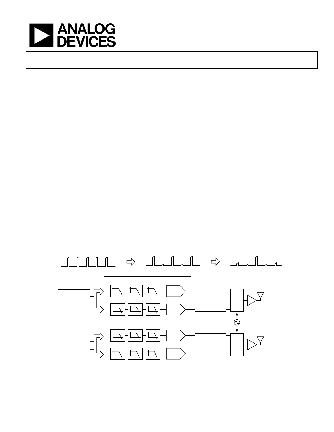
COMPLEX BASEBAND
TYPICAL SIGNAL CHAIN
COMPLEX IF
RF
DC
FPGA/ASIC/DSP
fIF
DIGITAL INTERPOLATION FILTERS
↑2 ↑2 ↑2
DAC1
↑2 ↑2 ↑2
DAC2
LO ± fIF
POST DAC
ANALOG FILTER
AQM
LO
PA
↑2 ↑2 ↑2
DAC3
↑2 ↑2 ↑2
DAC4
POST DAC
LO
AQM
PA
NOTES
1. AQM = ANALOG QUADRATURE MODULATOR.
Figure 1.
Rev. B
Information furnished by Analog Devices is believed to be accurate and reliable. However, no
responsibility is assumed by Analog Devices for its use, nor for any infringements of patents or other
rights of third parties that may result from its use. Specifications subject to change without notice. No
license is granted by implication or otherwise under any patent or patent rights of Analog Devices.
Trademarksandregisteredtrademarksarethepropertyoftheirrespectiveowners.
One Technology Way, P.O. Box 9106, Norwood, MA 02062-9106, U.S.A.
Tel: 781.329.4700
www.analog.com
Fax: 781.461.3113 ©2010–2012 Analog Devices, Inc. All rights reserved.
1 page 
AD9148
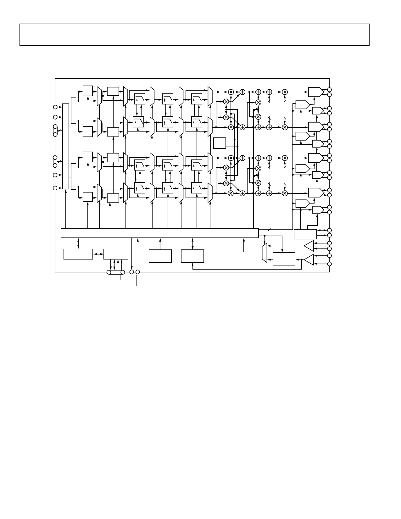
FUNCTIONAL BLOCK DIAGRAM
Data Sheet
DCIA_P/
DCIA_N
FRAMEA_P/
FRAMEA_N
1.2GHz
A[15:0]_P/ 16
A[15:0]_N
310MHz
fS/2
MOD
fS/2
MOD
B[15:0]_P/ 16
B[15:0]_N
FRAMEB_P/
FRAMEB_N
DCIB_P/
DCIB_N
fS/2
MOD
fS/2
MOD
PROGRAMMING
REGISTERS
310MHz
SINC–1
310MHz/620MHz
2×
500MHz/1GHz
2×
500MHz/1GHz
2×
SINC–1
2×
SINC–1
2×
2×
2×
2×
COS
32-BIT
NCO SIN
2×
SINC–1
2×
2×
2×
INTERNAL CLOCK TIMING AND CONTROL LOGIC
SERIAL
IN/OUT PORT
POWER-ON
RESET
MULTI-CHIP
SYNC
SYNC
1GHz
16-BIT
DAC1
I OFFSET I GAIN
Q OFFSET Q GAIN
GAIN
AUX1
16-BIT
DAC2
GAIN
AUX2
16-BIT
DAC3
I OFFSET I GAIN
Q OFFSET Q GAIN
GAIN
AUX3
16-BIT
DAC4
GAIN
AUX4
GAIN/
OFFSET_CTR L
PLL_CTR L
REFERENCE
BIAS
DAC_CLK
CLOCK
MULTIPLIER
(2× – 16×)
IOUT1_P
IOUT1_N
AUX1_P
AUX1_N
IOUT2_P
IOUT2_N
AUX2_P
AUX2_N
IOUT3_P
IOUT3_N
AUX3_P
AUX3_N
IOUT4_P
IOUT4_N
AUX4_P
AUX4_N
VREF
I120
CLK_P
CLK_N
REFCLK_P/
SYNC_ P
REFCLK_N/
SYNC_N
Figure 2.
Rev. B | Page 4 of 72
5 Page 
AD9148
Table 8. Thermal Resistance and Maximum Power
PCB
Package Type
TA (°C) PCB Layers PCB Vias External Heat Sink1
196-ball CSP_BGA 85
12
25 No
196-ball CSP_BGA 85
12
25 Yes
196-ball BGA_ED 85
12
25 No
196-ball BGA_ED 85
12
25 Yes
1 Heat sink is used in the thermal model: 13 mm × 13 mm, 15 mm tall.
Case
CSP_BGA
CSP_BGA
BGA_ED
BGA_ED
Data Sheet
TJ (°C)
125
125
125
125
θJA (°C/W)
18.0
16.0
15.0
14.0
Maximum
Power (W)
2.22
2.50
2.67
2.86
Table 9. Power vs. fDAC Rate and Functionality
Maximum Power (W)
2.22
2.50
2.67
2.86
Package
CSP_BGA
CSP_BGA
BGA_EP
BGA_EP
Heat-Sink Combination2
No
Yes
No
Yes
1 Typical maximum fDAC rate with inverse sinc filter off.
2 Heat sink is used in the thermal model: 13 mm × 13 mm, 15 mm tall.
Maximum fDAC (MSPS)1
Coarse Modulation
Fine Modulation (NCO)
PLL Off
PLL On
PLL Off
PLL On
820 740 695
630
950 875 810
740
1000
945
870
810
1000
1000
940
870
Rev. B | Page 10 of 72
11 Page | ||
| Páginas | Total 30 Páginas | |
| PDF Descargar | [ Datasheet AD9148.PDF ] | |
Hoja de datos destacado
| Número de pieza | Descripción | Fabricantes |
| AD9142 | Digital-to-Analog Converter | Analog Devices |
| AD9142A | Digital-to-Analog Converter | Analog Devices |
| AD9144 | Digital-to-Analog Converter | Analog Devices |
| AD9146 | TxDAC Digital-to-Analog Converter | Analog Devices |
| Número de pieza | Descripción | Fabricantes |
| SLA6805M | High Voltage 3 phase Motor Driver IC. |
Sanken |
| SDC1742 | 12- and 14-Bit Hybrid Synchro / Resolver-to-Digital Converters. |
Analog Devices |
|
DataSheet.es es una pagina web que funciona como un repositorio de manuales o hoja de datos de muchos de los productos más populares, |
| DataSheet.es | 2020 | Privacy Policy | Contacto | Buscar |
