|
|
|
PDF 71M6533H Data sheet ( Hoja de datos )
| Número de pieza | 71M6533H | |
| Descripción | Energy Meter IC | |
| Fabricantes | TERIDIAN Semiconductor | |
| Logotipo | ||
Hay una vista previa y un enlace de descarga de 71M6533H (archivo pdf) en la parte inferior de esta página. Total 30 Páginas | ||
|
No Preview Available !
Simplifying System IntegrationTM
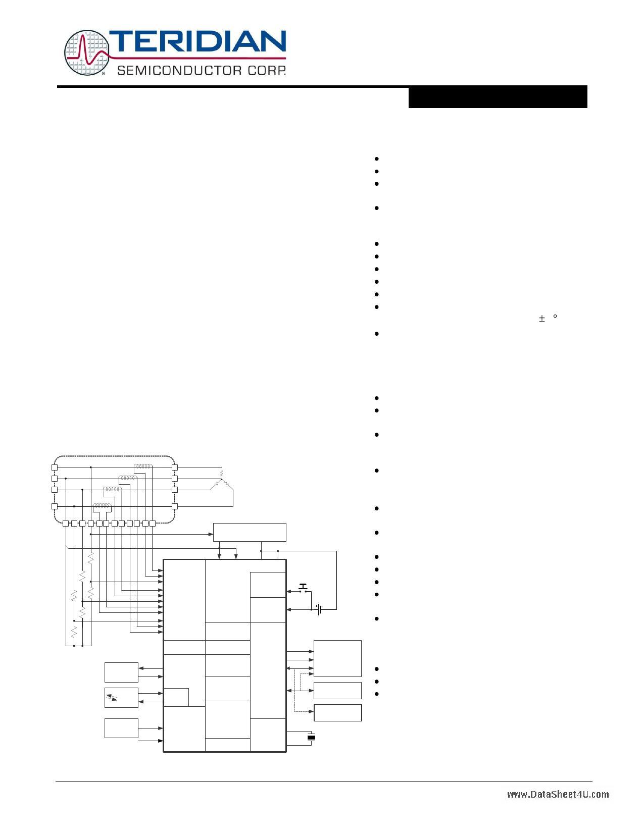
GENERAL DESCRIPTION
The 71M6533 and 71M6534 are Teridian’s 3rd-generation poly-
phase metering SOCs with a 10MHz 8051-compatible MPU
core, low-power RTC, FLASH and LCD driver. Teridian’s pa-
tented Single Converter Technology® with a 22-bit delta-sigma
ADC, seven analog inputs, digital temperature compensation,
precision voltage reference and a 32-bit computation engine
(CE) supports a wide range of metering applications with very
few external components.
The 71M6533 and 71M6534 add several new features to Teri-
dian’s flagship 71M6513 poly-phase meters including an SPI in-
terface, advanced power management with <1 µA sleep cur-
rent, 4 KB shared RAM and 128 KB (71M6533/H, 71M6534) or
256 KB (71M6534H) Flash which may be programmed in the
field with new code and/or data during meter operation. Higher
processing and sampling rates and larger memory offer a po-
werful metering platform for commercial and industrial meters
with up to class 0.2 accuracy.
A complete array of ICE and development tools, programming
libraries and reference designs enable rapid development and
certification of meters that meet all ANSI & IEC electricity meter-
ing standards worldwide.
LIVE
NEUT
LIVE
CT/ COIL
LIVE
AMR
IR
POWER
FAULT
LOAD
NEUTRAL
POWER SUPPLY
CONVERTER
IA
VA
IB
VB
IC
VC
ID
V3P3A V3P3SYS GNDA GNDD
TERIDIAN
71M6533
71M6534
PWR MODE
CONTROL
WAKE-up
REGULATOR
VBAT
V2P5
TEMP
SENSOR
LCD DRIVER
DIO ,PULSE
VREF
SERIAL PORTS
TX
RX
RAM
COMPUTE
ENGINE
COM0..3
SEG
SEG/ DIO
RX
MOD TX
COMPARATOR
V1
V2*
FLASH
MPU
RTC
TIMERS
ICE
DIO
OSC/ PLL
XIN
XOUT
* 71M6534 only
9/24/2008
BATTERY
8888.8888
PULSES,
DIO
I2C or µWire
EEPROM
32 kHz
www.DataSheet4U.com
71M6533/H and 71M6534/H
Energy Meter IC
DATA SHEET
November 2009
FEATURES
Accuracy < 0.1% over 2000:1 range
Exceeds IEC62053 / ANSI C12.20 standards
Seven sensor inputs with neutral current
measurement
Low-jitter Wh and VARh plus two additional
pulse test outputs (4 total, 10 kHz maximum)
with pulse count
Four-quadrant metering
Phase sequencing
Line frequency count for RTC
Digital temperature compensation
Independent 32-bit compute engine
46-64 Hz line frequency range with same
calibration. Phase compensation ( 7 )
Three battery back-up modes with wake-up
on timer or push-button:
Brownout mode (82 µA typ., 71M6533)
LCD mode (21 µA typ., DAC active)
Sleep mode (0.7 µA typ.)
Energy display during mains power failure
39 mW typical consumption @ 3.3 V, MPU
clock frequency 614 kHz
8-bit MPU (80515), 1 clock cycle per in-
struction, 10 MHz maximum, with integrated
ICE for debug
LCD driver with 4 common segment drivers:
Up to 228 (71M6533) or 300 (71M6534)
pixels
4 dedicated plus 35 (71M6533) or
48 (71M6534) multi-function DIO pins
RTC for TOU functions with clock-rate adjust
register
Hardware watchdog timer, power fail monitor
I2C/Microwire EEPROM Interface
High-speed slave SPI interface to data RAM
Two UARTs for IR and AMR, IR driver with
modulation
Flash memory with security and in-system
program update:
128 KB (71M6533/H, 71M6534)
256 KB (71M6534H)
4 KB RAM
Industrial temperature range
100-pin (71M6533/H) or 120-pin
(71M6534/H) lead free LQFP package
v1.1 © 2007-2009 TERIDIAN Semiconductor Corporation 1
1 page 
FDS_6533_6534_004
71M6533/71M653w4wDwa.DtaataSShheeete4Ut .com
Figures
Figure 1: IC Functional Block Diagram ......................................................................................................... 8
Figure 2: General Topology of a Chopped Amplifier .................................................................................. 12
Figure 3: CROSS Signal with CHOP_E = 00.............................................................................................. 13
Figure 4: AFE Block Diagram...................................................................................................................... 14
Figure 5: Samples from Multiplexer Cycle .................................................................................................. 17
Figure 6: Accumulation Interval................................................................................................................... 17
Figure 7: Interrupt Structure ........................................................................................................................ 36
Figure 8: Optical Interface........................................................................................................................... 42
Figure 9: Connecting an External Load to DIO Pins ................................................................................... 45
Figure 10: 3-wire Interface. Write Command, HiZ=0. ................................................................................ 48
Figure 11: 3-wire Interface. Write Command, HiZ=1 ................................................................................. 48
Figure 12: 3-wire Interface. Read Command............................................................................................. 48
Figure 13: 3-Wire Interface. Write Command when CNT=0 ...................................................................... 49
Figure 14: 3-wire Interface. Write Command when HiZ=1 and WFR=1. ................................................... 49
Figure 15: SPI Slave Port: Typical Read and Write operations .................................................................. 50
Figure 16: Functions defined by V1 ............................................................................................................ 51
Figure 17: Voltage, Current, Momentary and Accumulated Energy ........................................................... 53
Figure 18: Timing Relationship between ADC MUX and Compute Engine ................................................ 54
Figure 19: RTM Output Format ................................................................................................................... 54
Figure 20: Operation Modes State Diagram ............................................................................................... 55
Figure 21: Functional Blocks in BROWNOUT Mode .................................................................................. 58
Figure 22: Functional Blocks in LCD Mode................................................................................................. 59
Figure 23: Functional Blocks in SLEEP Mode ............................................................................................ 60
Figure 24: Transition from BROWNOUT to MISSION Mode when System Power Returns ...................... 61
Figure 25: Power-Up Timing with V3P3SYS and VBAT tied together ........................................................ 61
Figure 26: Power-Up Timing with VBAT only.............................................................................................. 62
Figure 27: Wake Up Timing ........................................................................................................................ 63
Figure 28: MPU/CE Data Flow.................................................................................................................... 64
Figure 29: MPU/CE Communication ........................................................................................................... 64
Figure 30: Resistive Voltage Divider ........................................................................................................... 65
Figure 31: CT with Single Ended (Left) and Differential Input (Right) Connection ..................................... 65
Figure 32: Resistive Shunt (Left), Rogowski Sensor (Right) ...................................................................... 65
Figure 33: Connecting LCDs....................................................................................................................... 68
Figure 34: I2C EEPROM Connection .......................................................................................................... 68
Figure 35: Three-Wire EEPROM Connection ............................................................................................. 69
Figure 36: Connections for UART0 ............................................................................................................. 69
Figure 37: Connection for Optical Components.......................................................................................... 70
Figure 38: Voltage Divider for V1 ................................................................................................................ 71
Figure 39: External Components for the RESET Pin: Push-Button (Left), Production Circuit (Right)........ 71
Figure 40: External Components for the Emulator Interface ...................................................................... 72
Figure 41: Connecting a Battery ................................................................................................................. 72
Figure 42: CE Data Flow: Multiplexer and ADC........................................................................................ 100
Figure 43: CE Data Flow: Scaling, Gain Control, Intermediate Variables ................................................ 100
Figure 44: CE Data Flow: Squaring and Summation Stages.................................................................... 101
Figure 45: SPI Slave Port (MISSION Mode) Timing ................................................................................. 111
Figure 46: Wh Accuracy (0.1 A - 200 A, 240 V, Room Temperature) at Various Frequencies (Differential
Mode, CTs) ........................................................................................................................................ 112
Figure 47: Typical Wh Accuracy (0.02 A - 200 A, 240 V, Room Temperature), Various Load Angles
(Differential Mode, CTs)..................................................................................................................... 112
Figure 48: 71M6533/6533H 100-pin LQFP Package Outline ................................................................... 113
Figure 49: 71M6534/6534H 120-pin LQFP Package Outline ................................................................... 114
Figure 50: Pinout for 71M6533/71M6533H LQFP-100 Package .............................................................. 115
Figure 51: Pinout for 71M6534/71M6534H LQFP-120 Package .............................................................. 116
v1.1
© 2007-2009 TERIDIAN Semiconductor Corporation
5
5 Page 
FDS_6533_6534_004
71M6533/71M653w4wDwa.DtaataSShheeete4Ut .com
cal assignment of values for the SLOTn_SEL and SLOTn_ALTSEL registers assuming seven time slots
(MUX_DIV = 7) for the processing of three voltage and current phases plus an additional neutral current.
The correlation between signal numbers, CE memory addresses, and analog signals is given in Table 3.
For the processing of three voltage and current phases in a typical poly-phase meter without neutral
measurement, MUX_DIV is set to 6, and SLOT6_SEL as well as SLOT6_ALTSEL would be empty.
Table 1: Signals Selected for the ADC with SLOTn_SEL and SLOTn_ALTSEL (MUX_DIV = 7)
Time Slot
0
1
2
3
4
5
6
Regular Slot
Register
Typical Selections
Signal Signal for
Number
ADC
SLOT0_SEL
SLOT1_SEL
0
1
IA
VA
SLOT2_SEL
2
IB
SLOT3_SEL
SLOT4_SEL
3
4
VB
IC
SLOT5_SEL
SLOT6_SEL
SLOT7_SEL
SLOT8_SEL
SLOT9_SEL
5
6
–
–
–
VC
ID
–
–
–
Alternate Slot
Register
Typical Selections
Signal Signal for
Number
ADC
SLOT0_ALTSEL
SLOT1_ALTSEL
A
1
TEMP
VA
SLOT2_ALTSEL
B
VBAT
SLOT3_ALTSEL
SLOT4_ALTSEL
3
4
VB
IC
SLOT5_ALTSEL
SLOT6_ALTSEL
5
6
VC
ID
SLOT7_ALTSEL
SLOT8_ALTSEL
SLOT9_ALTSEL
The duration of each multiplexer state depends on the number of ADC samples processed by the FIR,
which is set by FIR_LEN. Each multiplexer state will start on the rising edge of CK32. FIR conversions
require 1, 2, or 3 CK32 cycles. The number of CK32 cycles is determined by FIR_LEN.
1.2.3 A/D Converter (ADC)
A single delta-sigma A/D converter digitizes the voltage and current inputs to the 71M6533/71M6534. The
resolution of the ADC is programmable using the I/O RAM registers M40MHZ and M26MHZ (see Table 2).
Table 2: ADC Resolution
Setting for [M40MHZ,
M26MHZ]
[00], [10] or [11]
[01]
FIR_LEN FIR CE Cycles Resolution
0 138 18 bits
1 288 21 bits
2 384 22 bits
0 186 19 bits
1 384 22 bits
2 588 24 bits
Initiation of each ADC conversion is controlled by MUX_CTRL as described above. At the end of each ADC
conversion, the FIR filter output data is stored into the CE RAM location determined by the MUX selection.
1.2.4 FIR Filter
The finite impulse response filter is an integral part of the ADC and it is optimized for use with the multip-
lexer. The purpose of the FIR filter is to decimate the ADC output to the desired resolution. At the end of
each ADC conversion, the output data is stored into the fixed CE RAM location determined by the multip-
lexer selection as shown in Table 3. FIR data is stored LSB justified, but shifted left by eight bits.
v1.1
© 2007-2009 TERIDIAN Semiconductor Corporation
11
11 Page | ||
| Páginas | Total 30 Páginas | |
| PDF Descargar | [ Datasheet 71M6533H.PDF ] | |
Hoja de datos destacado
| Número de pieza | Descripción | Fabricantes |
| 71M6533 | Energy Meter IC | TERIDIAN Semiconductor |
| 71M6533H | Energy Meter IC | TERIDIAN Semiconductor |
| Número de pieza | Descripción | Fabricantes |
| SLA6805M | High Voltage 3 phase Motor Driver IC. |
Sanken |
| SDC1742 | 12- and 14-Bit Hybrid Synchro / Resolver-to-Digital Converters. |
Analog Devices |
|
DataSheet.es es una pagina web que funciona como un repositorio de manuales o hoja de datos de muchos de los productos más populares, |
| DataSheet.es | 2020 | Privacy Policy | Contacto | Buscar |