|
|
|
PDF AD5749 Data sheet ( Hoja de datos )
| Número de pieza | AD5749 | |
| Descripción | Industrial Current Out Drive | |
| Fabricantes | Analog Devices | |
| Logotipo | ||
Hay una vista previa y un enlace de descarga de AD5749 (archivo pdf) en la parte inferior de esta página. Total 29 Páginas | ||
|
No Preview Available !
Data Sheet
Industrial Current Out Driver, Single-Supply,
55 V Maximum Supply, Programmable Ranges
AD5749
FEATURES
Current output ranges: 0 mA to 24 mA or 4 mA to 20 mA
±0.03% FSR typical total unadjusted error (TUE)
±5 ppm/°C typical output drift
2% overrange
Flexible serial digital interface
On-chip output fault detection
PEC error checking
Asynchronous CLEAR function
Power supply range
AVDD: 12 V (± 10%) to 55 V (maximum)
Output loop compliance to AVDD − 2.75 V
Temperature range: −40°C to +105°C
32-lead, 5 mm × 5 mm LFCSP package
APPLICATIONS
Process control
Actuator control
PLCs
GENERAL DESCRIPTION
The AD5749 is a single channel, low cost, precision, current output
driver with hardware or software programmable output ranges.
The software ranges are configured via an SPI-/MICROWIRE™-
compatible serial interface. The AD5749 targets applications in
PLC and industrial process control. The analog input to the
AD5749 is provided from a low voltage, single-supply digital-to-
analog converter (DAC) and is internally conditioned to provide
the desired output current/voltage range.
The output current range is programmable across two current
ranges: 0 mA to 24 mA, or 4 mA to 20 mA. Current output is
open-circuit protected and can drive inductive loads of 0.1 H.
The device is specified to operate with a power supply range
from 10.8 V to 55 V. Output loop compliance is 0 V to AVDD −
2.75 V.
The flexible serial interface is SPI and MICROWIRE compatible
and can be operated in 3-wire mode to minimize the digital
isolation required in isolated applications. The interface also
features an optional PEC error checking feature using CRC-8
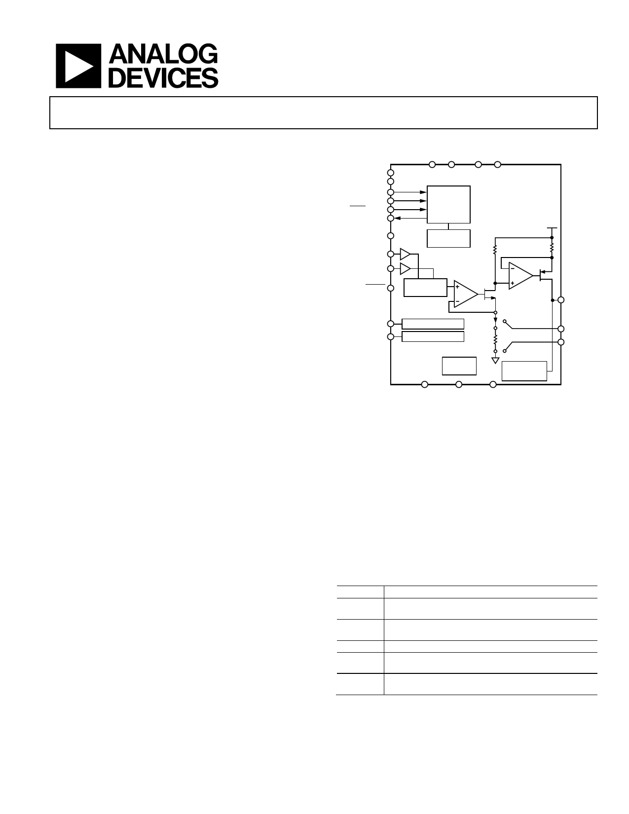
FUNCTIONAL BLOCK DIAGRAM
DVCC GND AVDD GND
CLEAR
CLRSEL
SCLK/OUTEN*
SDIN/R0*
SYNC/RSET*
SDO/VFAULT*
HW SELECT
VIN
INPUT SHIFT
REGISTER
AND
CONTROL
LOGIC
AD5749
AVDD
STATUS
REGISTER
R2
R3
VREF
RESET
IOUT RANGE
SCALING
IOUT
FAULT/TEMP*
NC/IFAULT*
OVERTEMP
IOUT OPEN FAULT
IOUT OPEN FAULT
RSET
POWER-
ON RESET
IOUT
OPEN FAULT
REXT1
REXT2
AD2/R1* AD1/R2* AD0/R3*
*DENOTES SHARED PIN. SOFTWARE MODE DENOTED BY REGULAR TEXT,
HARDWARE MODE DENOTED BY ITALIC TEXT. FOR EXAMPLE, FOR
FAULT/TEMP PIN, IN SOFTWARE MODE, THIS PIN TAKES ON FAULT
FUNCTION. IN HARDWARE MODE, THIS PIN TAKES ON TEMP FUNCTION.
Figure 1.
error checking, useful in industrial environments where data
communication corruption can occur.
The device also includes a power-on reset function ensuring
that the device powers up in a known state and an asynchron-
ous CLEAR pin that sets the outputs to the low end of the
selected current range.
An HW SELECT pin is used to configure the part for hardware
or software mode on power-up.
Table 1. Related Devices
Part No. Description
AD5750
Industrial current/voltage output (I/V) driver with
programmable ranges
AD5751
Industrial I/V output driver, single-supply, 55 V maximum
supply, programmable ranges
AD5748 Industrial I/V output driver with programmable ranges
AD5410/
AD5420
Single-channel, 12-/16-bit, serial input, current source
output DAC
AD5412/
AD5422
Single-channel, 12-/16-bit, serial input, I/V output DAC
Rev. B
Document Feedback
Information furnished by Analog Devices is believed to be accurate and reliable. However, no
responsibility is assumed by Analog Devices for its use, nor for any infringements of patents or other
rights of third parties that may result from its use. Specifications subject to change without notice. No
license is granted by implication or otherwise under any patent or patent rights of Analog Devices.
Trademarksandregisteredtrademarksarethepropertyoftheirrespectiveowners.
One Technology Way, P.O. Box 9106, Norwood, MA 02062-9106, U.S.A.
Tel: 781.329.4700 ©2010–2013 Analog Devices, Inc. All rights reserved.
Technical Support
www.analog.com
1 page 
AD5749
Parameter1
OUTPUT CHARACTERISTICS2
Current Loop Compliance
Voltage
Resistive Load
Inductive Load
Settling Time
4 mA to 20 mA, Full-Scale
Step
120 µA Step, 4 mA to
20 mA Range
DC PSRR
Output Impedance
DIGITAL INPUTS2
Input High Voltage, VIH
Input Low Voltage, VIL
Input Current
Pin Capacitance
DIGITAL OUTPUTS2
FAULT, IFAULT, TEMP, VFAULT
VOL, Output Low Voltage
VOH, Output High Voltage
SDO
VOL, Output Low Voltage
VOH, Output High Voltage
High Impedance Output
Capacitance
High Impedance Leakage
Current
POWER REQUIREMENTS
AVDD
DVCC
Input Voltage
AIDD
Min Typ Max
0 AVDD − 2.75
See the Test Conditions/
Comments column
8.5
1.2
1
130
2
−1
5
0.8
+1
0.4
0.6
3.6
0.5
DVCC − 0.5
0.5
DVCC − 0.5
3
−1 +1
10.8
2.7
4.4
55
5.5
5.6
Unit
V
H
µs
µs
µA/V
MΩ
V
V
µA
pF
V
V
V
V
V
pF
µA
V
V
mA
DICC
Power Dissipation
5.2 6.2
0.3 1
108
mA
mA
mW
1 Temperature range: −40°C to +105°C; typical at +25°C.
2 Guaranteed by design and characterization, not production tested.
Data Sheet
Test Conditions/Comments
Chosen such that compliance is not exceeded
Needs appropriate capacitor at higher inductance
values; see the Driving Inductive Loads section
250 Ω load
250 Ω load
JEDEC compliant
Per pin
Per pin
10 kΩ pull-up resistor to DVCC
At 2.5 mA
10 kΩ pull-up resistor to DVCC
Sinking 200 µA
Sourcing 200 µA
Output unloaded, output disabled;
R3, R2, R1, R0 = 0000, RSET = 0
Output enabled
VIH = DVCC, VIL = GND
AVDD = 24 V, output unloaded
Rev. B | Page 4 of 28
5 Page 
AD5749
TYPICAL PERFORMANCE CHARACTERISTICS
Data Sheet
0.005
0.004
0.003
0.002
0.001
0
–0.001
–0.002
–0.003
–0.004
–0.005
4mA TO 20mA EXTERNAL RSET RESISTOR
0mA TO 24mA EXTERNAL RSET RESISTOR
VIN (V)
Figure 5. Integral Nonlinearity Error vs. VIN, External RSET Resistor
0.005
0.004
0.003
0.002
0.001
0
–0.001
–0.002
–0.003
–0.004
–0.005
4mA TO 20mA INTERNAL RSET RESISTOR
0mA TO 24mA INTERNAL RSET RESISTOR
VIN (V)
Figure 6. Integral Nonlinearity Error vs. VIN, Internal RSET Resistor
0.010
0.008
0.006
0.004
0.002
0
–0.002
–0.004
–0.006
–0.008
–0.010
4mA TO 20mA EXTERNAL RSET LINEARITY
0mA TO 24mA EXTERNAL RSET LINEARITY
24V 48V 55V
SUPPLY VOLTAGE (AVDD)
Figure 7. Integral Nonlinearity Current Mode, External RSET Sense Resistor
0.010
0.008
0.006
0.004
0.002
0
–0.002
–0.004
–0.006
–0.008
–0.010
4mA TO 20mA INTERNAL RSET LINEARITY
0mA TO 24mA INTERNAL RSET LINEARITY
24V 48V 55V
SUPPLY VOLTAGE (AVDD)
Figure 8. Integral Nonlinearity Current Mode, Internal RSET Sense Resistor
0.05
0.04
0.03
0.02
0.01
0
–0.01
–0.02
–0.03
–0.04
–0.05
4mA TO 20mA EXTERNAL RSET TUE
0mA TO 24mA EXTERNAL RSET TUE
VIN (V)
Figure 9. Total Unadjusted Error vs. VIN, External RSET Resistor
0.05
0.04
0.03
0.02
0.01
0
–0.01
–0.02
–0.03
–0.04
–0.05
4mA TO 20mA INTERNAL RSET TUE
0mA TO 24mA INTERNAL RSET TUE
VIN (V)
Figure 10. Total Unadjusted Error vs. VIN, Internal RSET Resistor
Rev. B | Page 10 of 28
11 Page | ||
| Páginas | Total 29 Páginas | |
| PDF Descargar | [ Datasheet AD5749.PDF ] | |
Hoja de datos destacado
| Número de pieza | Descripción | Fabricantes |
| AD574 | Complete 12-Bit A/D Converter | Analog Devices |
| AD5744 | (AD5744 / AD5764) Bipolar Voltage Output DAC | Analog Devices |
| AD5744R | Bipolar Voltage Output DAC | Analog Devices |
| AD5748 | Industrial Current/Voltage Output Driver | Analog Devices |
| Número de pieza | Descripción | Fabricantes |
| SLA6805M | High Voltage 3 phase Motor Driver IC. |
Sanken |
| SDC1742 | 12- and 14-Bit Hybrid Synchro / Resolver-to-Digital Converters. |
Analog Devices |
|
DataSheet.es es una pagina web que funciona como un repositorio de manuales o hoja de datos de muchos de los productos más populares, |
| DataSheet.es | 2020 | Privacy Policy | Contacto | Buscar |