|
|
|
PDF LMZ10504 Data sheet ( Hoja de datos )
| Número de pieza | LMZ10504 | |
| Descripción | 4A SIMPLE SWITCHER Power Module | |
| Fabricantes | National Semiconductor | |
| Logotipo | ||
Hay una vista previa y un enlace de descarga de LMZ10504 (archivo pdf) en la parte inferior de esta página. Total 22 Páginas | ||
|
No Preview Available !
DataSheet.in
LMZ10504
March 30, 2010
4A SIMPLE SWITCHER® Power Module with 5.5V Maximum
Input Voltage
Easy to Use 7 Pin Package
Performance Benefits
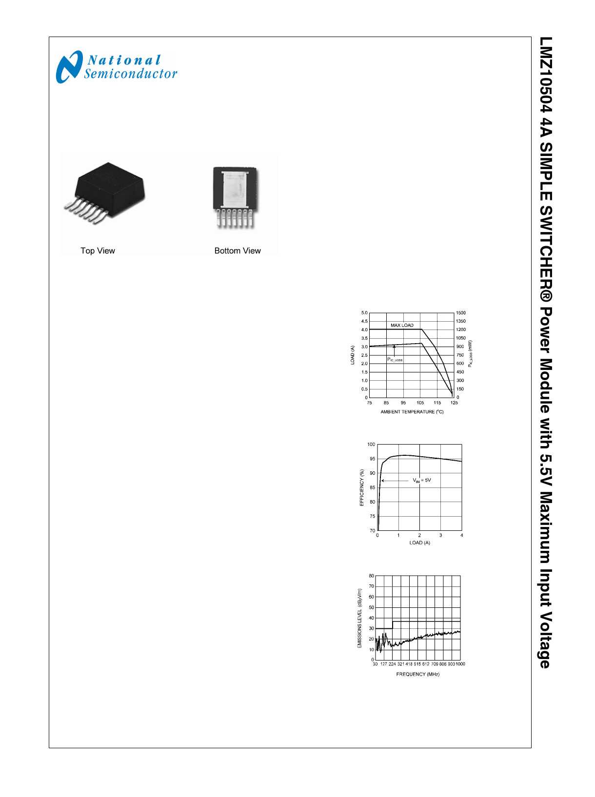
TO-PMOD 7 Pin Package
300882a4
10.16 x 13.77 x 4.57 mm (0.4 x 0.39 x 0.18 in)
θJA = 20°C/W, θJC = 1.9°C/W (Note 1)
RoHS Compliant
■ Operates at high ambient temperatures
■ High efficiency up to 96% reduces system heat generation
■ Low radiated emissions (EMI) complies with EN55022
class B standard (Note 2)
■ Passes 10V/m radiated immunity EMI test standard
EN61000 4-3
■ Low output voltage ripple of 10 mV allows for powering
noise-sensitive transceiver and signaling ICs
■ Fast transient response for powering FPGAs and ASICs
System Performance
Current Derating (VOUT = 3.3V)
Electrical Specifications
■ 20W maximum total output power
■ Up to 4A output current
■ Input voltage range 2.95V to 5.5V
■ Output voltage range 0.8V to 5V
■ ±1.63% feedback voltage accuracy over temperature
■ Efficiency up to 96%
Key Features
■ Integrated shielded inductor
■ Flexible startup sequencing using external soft-start,
tracking, and precision enable
■ Protection against in-rush currents and faults such as input
UVLO and output short-circuit
■ -40°C to +125°C junction temperature operating range
■ Single exposed pad and standard pinout for easy
mounting and manufacturing
■ Pin-to-pin compatible with
LMZ10503 (3A/15W max)
LMZ10505 (5A/25W max)
■ Fully enable for WEBENCH® and Power Designer
300882a5
Efficiency (VOUT = 3.3V)
300882a6
Radiated Emissions (EN 55022, Class B)
Applications
■ Point-of-load conversions from 3.3V and 5V rails
■ Space constrained applications
■ Extreme temperatures/no air flow environments
■ Noise sensitive applications (i.e. transceiver, medical)
300882a7
Note 1: θ JA measured on a 2.25” x 2.25” (5.8 cm x 5.8 cm) four layer board. Refer to PCB Layout Diagrams or Evaluation
Board Application Note: AN-2022.
Note 2: EN 55022:2006, +A1:2007, FCC Part 15 Subpart B: 2007. See Figure 5 and layout for information on device under
test.
© 2010 National Semiconductor Corporation 300882
www.national.com
1 page 
DataSheet.in
Typical Performance Characteristics Unless otherwise specified, the following conditions apply: VIN =
VEN = 5.0V, CIN is 47 µF 10V X5R ceramic capacitor; TAMBIENT = 25°C for efficiency curves and waveforms.
Load Transient Response
VIN = 3.3V, VOUT = 2.5V, IOUT = 0.4A to 3.6A to 0.4A step
20 mV/DIV, 20 MHz Bandwidth Limited
Refer to Table 5 for BOM, includes optional components
Load Transient Response
VIN = 5.0V, VOUT = 2.5V, IOUT = 0.4A to 3.6A to 0.4A step
20 mV/DIV, 20 MHz Bandwidth Limited
Refer to Table 5 for BOM, includes optional components
30088262
Output Voltage Ripple
VIN = 3.3V, VOUT = 2.5V, IOUT = 4A, 20 mV/DIV
Refer to Table 5 for BOM
30088263
Output Voltage Ripple
VIN = 5.0V, VOUT = 2.5V, IOUT = 4A, 20 mV/DIV
Refer to Table 5 for BOM
30088264
30088265
5 www.national.com
5 Page 
DataSheet.in
Estimate Power Dissipation And
Board Thermal Requirements
Use the current derating curves in the typical performance
characteristics section to obtain an estimate of power loss
(PIC_LOSS). For the design case of VIN = 5V, VOUT = 2.5V,
IOUT = 4A, TA(MAX) = 85°C , and TJ(MAX) = 125°C, the device
must see a thermal resistance from case to ambient (θCA) of
less than:
Given the typical thermal resistance from junction to case
(θJC) to be 1.9°C/W (typ.). Continuously operating at a TJ
greater than 125°C will have a shorten life span.
To reach θCA = 41°C/W, the PCB is required to dissipate heat
effectively. With no airflow and no external heat, a good esti-
mate of the required board area covered by 1oz. copper on
both the top and bottom metal layers is:
As a result, approximately 12 square cm of 1oz. copper on
top and bottom layers is required for the PCB design.
The PCB copper heat sink must be connected to the exposed
pad (EP). Approximately thirty six, 10mils (254 μm) thermal
vias spaced 59mils (1.5 mm) apart must connect the top cop-
per to the bottom copper. For an extended discussion and
formulations of thermal rules of thumb, refer to AN-2020 and
for an example of a high thermal performance PCB layout,
refer to the evaluation board application note AN-2022.
PC Board Layout Guidelines
PC board layout is an important part of DC-DC converter de-
sign. Poor board layout can disrupt the performance of a DC-
DC converter and surrounding circuitry by contributing to EMI,
ground bounce and resistive voltage drop in the traces. These
can send erroneous signals to the DC-DC converter resulting
in poor regulation or instability. Good layout can be imple-
mented by following a few simple design rules.
FIGURE 1. High Current Loops
30088253
1. Minimize area of switched current loops.
From an EMI reduction standpoint, it is imperative to minimize
the high di/dt current paths. The high current that does not
overlap contains high di/dt, see Figure 1. Therefore physically
place input capacitor (Cin1) as close as possible to the
LMZ10504 VIN pin and GND exposed pad to avoid observ-
able high frequency noise on the output pin. This will minimize
the high di/dt area and reduce radiated EMI. Additionally,
grounding for both the input and output capacitor should con-
sist of a localized top side plane that connects to the GND
exposed pad (EP).
2. Have a single point ground.
The ground connections for the feedback, soft-start, and en-
able components should be routed only to the GND pin of the
device. This prevents any switched or load currents from
flowing in the analog ground traces. If not properly placed,
poor grounding can result in degraded load regulation or er-
ratic output voltage ripple behavior. Provide the single point
ground connection from pin 4 to EP.
3. Minimize trace length to the FB pin.
Both feedback resistors, Rfbt and Rfbb, and the compensation
components, Rcomp and Ccomp, should be located close to the
FB pin. Since the FB node is high impedance, keep the copper
area as small as possible. This is most important as relatively
high value resistors are used to set the output voltage.
4. Make input and output bus connections as wide as
possible.
This reduces any voltage drops on the input or output of the
converter and maximizes efficiency. To optimize voltage ac-
curacy at the load, ensure that a separate feedback voltage
sense trace is made at the load. Doing so will correct for volt-
age drops and provide optimum output accuracy.
5. Provide adequate device heat-sinking.
Use an array of heat-sinking vias to connect the exposed pad
to the ground plane on the bottom PCB layer. If the PCB has
multiple copper layers, thermal vias can also be employed to
make connection to inner layer heat-spreading ground
planes. For best results use a 6 x 6 via array with minimum
via diameter of 10mils (254 μm) thermal vias spaced 59mils
(1.5 mm). Ensure enough copper area is used for heat-sinking
to keep the junction temperature below 125°C.
11 www.national.com
11 Page | ||
| Páginas | Total 22 Páginas | |
| PDF Descargar | [ Datasheet LMZ10504.PDF ] | |
Hoja de datos destacado
| Número de pieza | Descripción | Fabricantes |
| LMZ10500 | LMZ10500 650-mA SIMPLE SWITCHER Nano Module With 5.5-V Maximum Input Voltage (Rev. F) | Texas Instruments |
| LMZ10500 | 650mA SIMPLE SWITCHER Nano Module | National Semiconductor |
| LMZ10501 | LMZ10501 1-A SIMPLE SWITCHER Nano Module With 5.5-V Maximum Input Voltage (Rev. F) | Texas Instruments |
| LMZ10501 | 1A SIMPLE SWITCHER Nano Module | National Semiconductor |
| Número de pieza | Descripción | Fabricantes |
| SLA6805M | High Voltage 3 phase Motor Driver IC. |
Sanken |
| SDC1742 | 12- and 14-Bit Hybrid Synchro / Resolver-to-Digital Converters. |
Analog Devices |
|
DataSheet.es es una pagina web que funciona como un repositorio de manuales o hoja de datos de muchos de los productos más populares, |
| DataSheet.es | 2020 | Privacy Policy | Contacto | Buscar |