|
|
|
PDF ZNBG4003 Data sheet ( Hoja de datos )
| Número de pieza | ZNBG4003 | |
| Descripción | 4 STAGE FET LNA BIAS CONTROLLER | |
| Fabricantes | Diodes Incorporated | |
| Logotipo | ||
Hay una vista previa y un enlace de descarga de ZNBG4003 (archivo pdf) en la parte inferior de esta página. Total 7 Páginas | ||
|
No Preview Available !
DataSheet.in
A Product Line of
Diodes Incorporated
ZNBG4003
4 STAGE FET LNA BIAS CONTROLLER
Summary
The ZNBG4003 is a four stage depletion mode FET bias controller intended primarily for satellite Low Noise Block’s (LNB’s), but
its also suitable for other LNA applications such as those in found in PMR’s and microwave links. The ZNBG4003 provides each
FET with a negative gate voltage and positive drain voltage with user programmable drain current.
Features
• Four stage FET bias controller
• Operating range of 5.0V to 8.0V
• FET drain voltages set at 2.0V
• FET drain current selectable from 0 to 15mA
• Allows first and second stage FETs to be run at different
(optimum) drain currents
• FET drain voltages and currents stable over temperature
• FETs protected against overstress during power-up and
power-down.
• Internal negative supply generator allowing single supply
operation (available for external use)
• Low external component count
Pin Assignments
D2
G2
VCC
GND
Top View
CSUB
G3
D4
G4
RCAL1
Applications
• Two single type Twin LNB’s
• Twin LNB’s
• Quad LNB’s
• Microwave links
• PMR and Cellular telephone systems
Bottom View
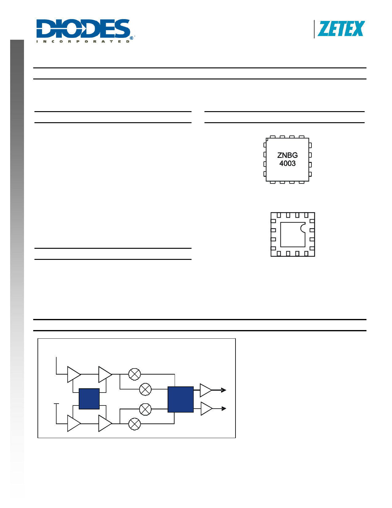
Single Universal LNB System Diagram
Gain stages
GaAs FET’s
Down
Converter
IF Switching, gain
and control
ZANBG
460023
ZXHF
5002
ZNBG4003
Document number: DS35007 Rev. 1 - 2
1 of 7
www.diodes.com
August 2010
© Diodes Incorporated
1 page 
DataSheet.in
A Product Line of
Diodes Incorporated
ZNBG4003
Applications Information
Above is a partial applications circuit for the ZNBG4003 showing all external components needed for biasing one of the four FET
stages available. Each bias stage is provided with a gate and drain pin. The drain pin provides a regulated 2.0V supply that
includes a drain current monitor. The drain current taken by the external FET is compared with a user selected level, generating a
signal that adjusts the gate voltage of the FET to obtain the required drain current. If for any reason, an attempt is made to draw
more than the user set drain current from the drain pin, the drain voltage will be reduced to ensure excess current is not taken.
The gate pin drivers are also current limited.
The bias stages are split up into two pairs, with the drain current of each pair set by an external RCAL resistor. RCAL1 sets the drain
currents of stages 1 and 3, whilst RCAL2 sets the drain currents of stages 2 and 4. This allows the optimisation of drain currents for
differing tasks such as input stages where noise can be critical and later amplifier stages where gain may be more important.
A graph showing the relationship between the value of RCAL and ID is provided in the Typical Characteristics section of this
datasheet.
The ZNBG4003 includes a switched capacitor DC-DC converter that is used to generate the negative supply required to bias
depletion mode FETs used in common source circuit configuration as shown above. This converter uses two external capacitors,
CNB the charge transfer capacitor and CSUB the output reservoir capacitor. The circuit provides a regulated -2.5V supply both for
gate driver use and for external use if required (for extra discrete bias stages, mixer bias, local oscillator bias etc.). The -2.5V
supply is available from the CSUB pin.
If any bias stages are not required, their gate and drain pins may be left open circuit. If all bias stages associated with an RCAL
resistor are not required, then this resistor may be omitted.
To ease PCB layout, the pinout for the ZNBG4003 includes two Vcc pins. These pins are internally connected so only one of the
pins needs to be powered for the device to function. It is probable that the extra pin will help avoid the need for trace cross-over
components or ground plane disruption from reverse side PCB links. Note that the exposed pad of the package must be either left
floating or connected to Csub.
Package Outline Dimensions
E
D
Pin #1 ID
E2
e
b
A1
A3
A
L
D2
QFN16 3x3
Dim Min Max
A 0.55 0.65
A1 0.00 0.05
A3 0.15 Typ
b 0.18 0.28
D 2.95 3.05
D2 1.40 1.60
e 0.50 BSC
E 2.95 3.05
E2 1.40 1.60
L 0.35 0.45
Z 0.625 Typ
All Dimensions in mm
Z
Note: Controlling dimensions are in millimetres. Approximate dimensions are provided in inches.
The package appearance may vary as shown, for further details please contact your local Diodes sales office.
ZNBG4003
Document number: DS35007 Rev. 1 - 2
5 of 7
www.diodes.com
August 2010
© Diodes Incorporated
5 Page | ||
| Páginas | Total 7 Páginas | |
| PDF Descargar | [ Datasheet ZNBG4003.PDF ] | |
Hoja de datos destacado
| Número de pieza | Descripción | Fabricantes |
| ZNBG4000 | FET BIAS CONTROLLER | Zetex Semiconductors |
| ZNBG4001 | FET BIAS CONTROLLER | Zetex Semiconductors |
| ZNBG4003 | 4 STAGE FET LNA BIAS CONTROLLER | Diodes Incorporated |
| Número de pieza | Descripción | Fabricantes |
| SLA6805M | High Voltage 3 phase Motor Driver IC. |
Sanken |
| SDC1742 | 12- and 14-Bit Hybrid Synchro / Resolver-to-Digital Converters. |
Analog Devices |
|
DataSheet.es es una pagina web que funciona como un repositorio de manuales o hoja de datos de muchos de los productos más populares, |
| DataSheet.es | 2020 | Privacy Policy | Contacto | Buscar |