|
|
|
PDF LM5035A Data sheet ( Hoja de datos )
| Número de pieza | LM5035A | |
| Descripción | PWM Controller | |
| Fabricantes | National Semiconductor | |
| Logotipo | ||
Hay una vista previa y un enlace de descarga de LM5035A (archivo pdf) en la parte inferior de esta página. Total 30 Páginas | ||
|
No Preview Available !
LM5035A/LM5035A-1
July 30, 2010
PWM Controller with Integrated Half-Bridge and SyncFET
Drivers
General Description
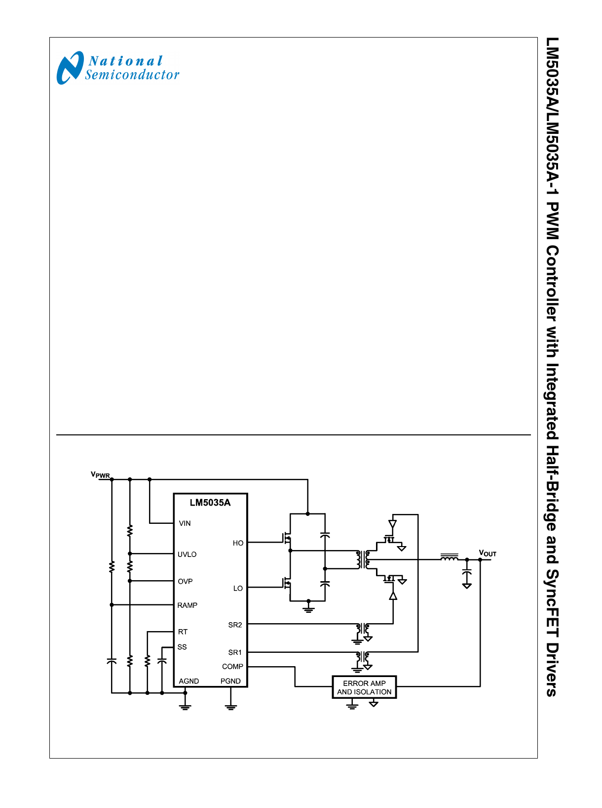
The LM5035A Half-Bridge Controller/Gate Driver contains all
of the features necessary to implement half-bridge topology
power converters using voltage mode control with line voltage
feed-forward. The LM5035A is a functional variant of the
LM5035 half-bridge PWM controller. The VCC current limit
threshold has been increased to 35 mA. The soft start and
soft start currents have been increased from 50 µA to 100 µA.
The BST UV threshold has been lowered to less than the VCC
UV threshold. The ratio of the T1 and T2 delays on the SR1
and SR2 outputs has been increased from 2:1 to 3:1. The
floating high-side gate driver is capable of operating with sup-
ply voltages up to 105V. Both the high-side and low-side gate
drivers are capable of 2A peak. An internal high voltage start-
up regulator is included, along with programmable line un-
dervoltage lockout (UVLO) and overvoltage protection (OVP).
The oscillator is programmed with a single resistor to fre-
quencies up to 2MHz. The oscillator can also be synchronized
to an external clock. A current sense input and a pro-
grammable timer provide cycle-by-cycle current limit and ad-
justable hiccup mode overload protection. The differences
between LM5035, LM5035A, LM5035B, and LM5035C are
summarized in Table 2.
Features
■ 105V / 2A Half-Bridge Gate Drivers
■ Synchronous Rectifier Control Outputs with
Programmable Delays
■ High Voltage (105V) Start-up Regulator
■ Voltage mode Control with Line Feed-Forward and Volt •
Second Limiting
■ Resistor Programmed, 2MHz Capable Oscillator
■ Patent Pending Oscillator Synchronization
■ Programmable Line Under-Voltage Lockout
■ Line Over-Voltage Protection
■ Internal Thermal Shutdown Protection
■ Adjustable Soft-Start
■ Versatile Dual Mode Over-Current Protection with Hiccup
Delay Timer
■ Cycle-by-Cycle Over-Current Protection
■ Direct Opto-coupler Interface
■ 5V Reference Output
Packages
■ TSSOP-20EP
■ LLP-24 (4mm x 5mm)
■ TSSOP-28EP (LM5035A-1 only)
Simplified Application Diagram
© 2010 National Semiconductor Corporation 300341
www.DataSheet.in
30034101
www.national.com
1 page 
TSSOP 20 PIN
LM5035A
5
LLP PIN
LM5035A
4
TSSOP 28 PIN
LM5035A-1
9
6 5 10
7 6 11
8 7 12
9 8 13
10 9 14
11 11 15
12 12 16
13 13 17
14 14 19
15 15 20
Name
RT
AGND
CS
SS
DLY
RES
HB
HS
HO
LO
PGND
Description
Application Information
Oscillator Frequency
Control and Sync Clock
Input
Normally biased at 2V. An external
resistor connected between RT
and AGND sets the internal
oscillator frequency. The internal
oscillator can be synchronized to
an external clock with a frequency
higher than the free running
frequency set by the RT resistor.
Analog Ground
Connect directly to Power Ground.
Current Sense input for
current limit
If CS exceeds 0.25V, the output
pulse will be terminated, entering
cycle-by-cycle current limit. An
internal switch holds CS low for
50ns after HO or LO switches high
to blank leading edge transients.
Soft-start Input
An internal 110µA current source
charges an external capacitor to
set the soft-start rate. During a
current limit restart sequence, the
internal current source is reduced
to 1.2µA to increase the delay
before retry.
Timing programming pin An external resistor to ground sets
for the LO and HO to SR1 the timing for the non-overlap time
and SR2 outputs.
of HO to SR1 and LO to SR2.
Restart Timer
If cycle-by-cycle current limit is
exceeded during any cycle, a 22 µA
current is sourced to the RES pin
capacitor.If the RES capacitor
voltage reaches 2.5V, the soft-start
capacitor will be fully discharged
and then released with a pull-up
current of 1.2µA. After the first
output pulse at LO (when SS
>COMP offset, typically 1V), the SS
pin charging current will revert to
110µA.
Boost voltage for the HO
driver
An external diode is required from
VCC to HB and an external
capacitor is required from HS to HB
to power the HO gate driver.
Switch node
Connection common to the
transformer and both power
switches. Provides a return path for
the HO gate driver.
High side gate drive
output.
Output of the high side PWM gate
driver. Capable of sinking 2A peak
current
Low side gate dfrive
output.
Output of the low side PWM gate
driver. Capable of sinking 2A peak
current.
Power Ground
Connect directly to Analog Ground.
www.DataSheet.in
5 www.national.com
5 Page 
Effective Comp Input Impedance
RDLY vs Deadtime
30034111
SR "T1" Parameter vs Temperature
30034112
SR "T2" Parameter vs Temperature
30034113
30034114
www.DataSheet.in
11 www.national.com
11 Page | ||
| Páginas | Total 30 Páginas | |
| PDF Descargar | [ Datasheet LM5035A.PDF ] | |
Hoja de datos destacado
| Número de pieza | Descripción | Fabricantes |
| LM5035 | Half-Bridge and SyncFET Drivers (Rev. H) | Texas Instruments |
| LM5035 | PWM Controller with Integrated Half-Bridge and SyncFET Drivers | National Semiconductor |
| LM5035A | LM5035A/5035A-1 PWM Controller with Integrated Half-Bridge SyncFET Drivers (Rev. F) | Texas Instruments |
| LM5035A | PWM Controller | National Semiconductor |
| Número de pieza | Descripción | Fabricantes |
| SLA6805M | High Voltage 3 phase Motor Driver IC. |
Sanken |
| SDC1742 | 12- and 14-Bit Hybrid Synchro / Resolver-to-Digital Converters. |
Analog Devices |
|
DataSheet.es es una pagina web que funciona como un repositorio de manuales o hoja de datos de muchos de los productos más populares, |
| DataSheet.es | 2020 | Privacy Policy | Contacto | Buscar |