|
|
|
PDF NLX1G10 Data sheet ( Hoja de datos )
| Número de pieza | NLX1G10 | |
| Descripción | 3-Input NAND Gate | |
| Fabricantes | ON Semiconductor | |
| Logotipo | ||
Hay una vista previa y un enlace de descarga de NLX1G10 (archivo pdf) en la parte inferior de esta página. Total 8 Páginas | ||
|
No Preview Available !
NLX1G10
3-Input NAND Gate
The NLX1G10 is an advanced high−speed 3−input CMOS NAND
gate in ultra−small footprint.
The NLX1G10 input structures provide protection when voltages up
to 7.0 V are applied, regardless of the supply voltage.
Features
• High Speed: tPD = 2.4 ns (Typ) @ VCC = 5.0 V
• Designed for 1.65 V to 5.5 V VCC Operation
• Low Power Dissipation: ICC = 1 mA (Max) at TA = 25°C
• 24 mA Balanced Output Source and Sink Capability
• Balanced Propagation Delays
• Overvoltage Tolerant (OVT) Input Pins
• Ultra−Small Packages
• These are Pb−Free Devices
A1
6C
GND
2
5 VCC
B3
4Y
Figure 1. Pinout (Top View)
A
B &Y
C
Figure 2. Logic Symbol
http://onsemi.com
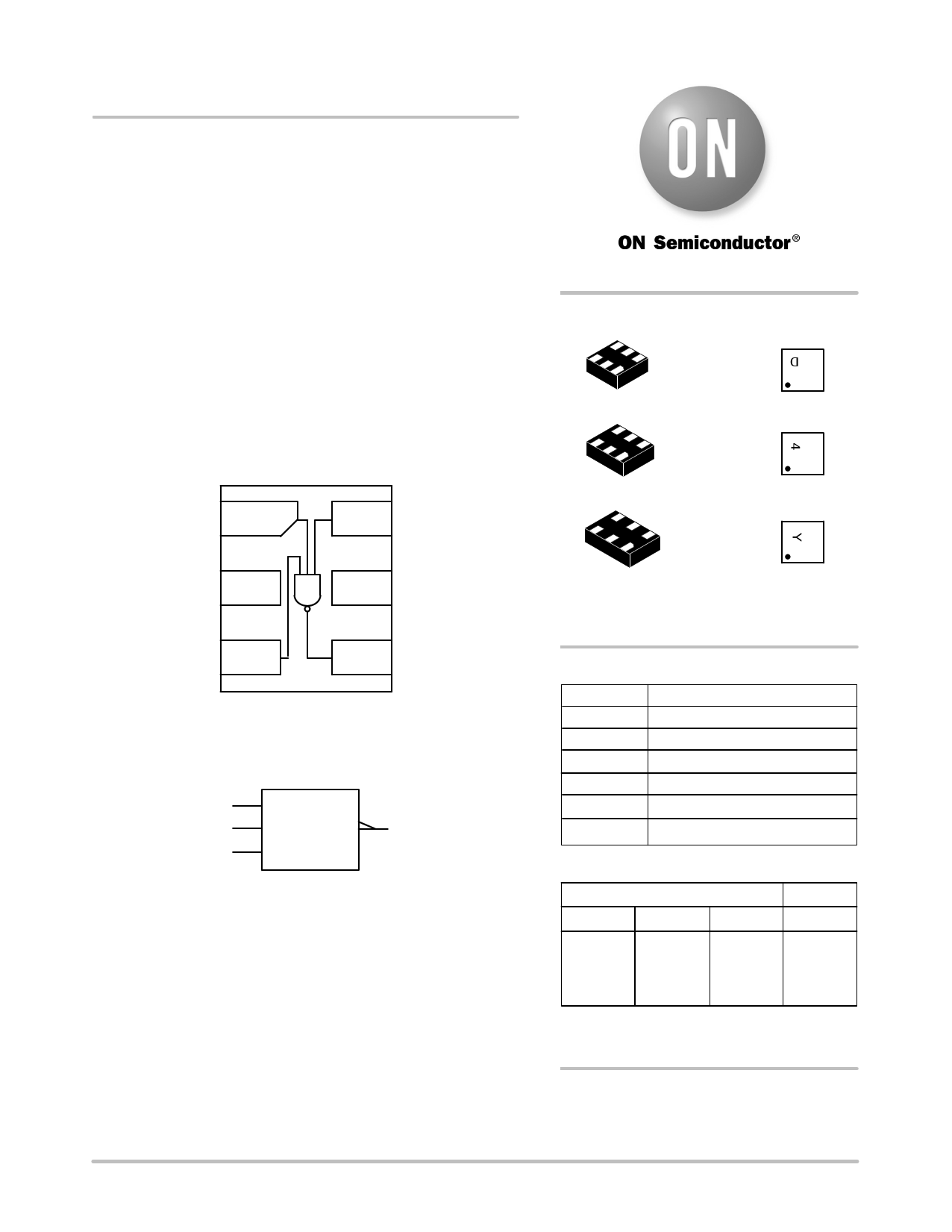
MARKING
DIAGRAMS
1
ULLGA6
1.0 x 1.0
CASE 613AD
M
G
1
ULLGA6
1.2 x 1.0
CASE 613AE
M
G
ULLGA6
1.45 x 1.0
M
CASE 613AF
G
1
X = Device Marking
M = Date Code
G = Pb−Free Package
PIN ASSIGNMENT
Pin Function
1A
2 GND
3B
4Y
5 VCC
6C
FUNCTION TABLE
Input
ABC
LXX
XLX
XX L
HHH
H − HIGH Logic Level
L − LOW Logic Level
X = Either LOW or HIGH Logic Level
Output
Y
H
H
H
L
ORDERING INFORMATION
See detailed ordering and shipping information in the package
dimensions section on page 5 of this data sheet.
© Semiconductor Components Industries, LLC, 2010
March, 2010 − Rev. 1
www.DataSheet.in
1
Publication Order Number:
NLX1G10/D
1 page 
NLX1G10
tR
INPUT
A and B
90%
50%
10%
90%
50%
tF
10%
VCC
GND
tPHL
tPLH
VOH
OUTPUT Y
50%
50%
VOL
tR = tF = 2.5 ns, 10% to 90%, f = 1 MHz, tW = 500 ns
Figure 3. Switching Waveforms
INPUT
OUTPUT
RL CL
A 1 MHz square input wave is recommended
for propagation delay tests
Figure 4. Test Circuit
ORDERING INFORMATION
Device
Package
Shipping†
NLX1G10AMX1TCG
ULLGA6, 1.45 x 1.0, 0.5P
(Pb−Free)
3000 / Tape & Reel
NLX1G10BMX1TCG
ULLGA6, 1.2 x 1.0, 0.4P
(Pb−Free)
3000 / Tape & Reel
NLX1G10CMX1TCG
ULLGA6, 1.0 x 1.0, 0.35P
(Pb−Free)
3000 / Tape & Reel
†For information on tape and reel specifications, including part orientation and tape sizes, please refer to our Tape and Reel Packaging
Specifications Brochure, BRD8011/D.
www.DataSheet.in
http://onsemi.com
5
5 Page | ||
| Páginas | Total 8 Páginas | |
| PDF Descargar | [ Datasheet NLX1G10.PDF ] | |
Hoja de datos destacado
| Número de pieza | Descripción | Fabricantes |
| NLX1G10 | 3-Input NAND Gate | ON Semiconductor |
| NLX1G11 | 3-Input AND Gate | ON Semiconductor |
| NLX1G125 | Non-Inverting 3-State Buffer | ON Semiconductor |
| Número de pieza | Descripción | Fabricantes |
| SLA6805M | High Voltage 3 phase Motor Driver IC. |
Sanken |
| SDC1742 | 12- and 14-Bit Hybrid Synchro / Resolver-to-Digital Converters. |
Analog Devices |
|
DataSheet.es es una pagina web que funciona como un repositorio de manuales o hoja de datos de muchos de los productos más populares, |
| DataSheet.es | 2020 | Privacy Policy | Contacto | Buscar |