|
|
|
PDF NLX1G99 Data sheet ( Hoja de datos )
| Número de pieza | NLX1G99 | |
| Descripción | Configurable Multifunction Gate | |
| Fabricantes | ON Semiconductor | |
| Logotipo | ||
Hay una vista previa y un enlace de descarga de NLX1G99 (archivo pdf) en la parte inferior de esta página. Total 15 Páginas | ||
|
No Preview Available !
NLX1G99
Configurable Multifunction
Gate
The NLX1G99 MiniGatet is an advanced high−speed CMOS
multifunction gate with a 3−state output. With the output enable input
(OE) at High, the output is disabled and is kept at high impedance.
With the output enable input (OE) at Low, the device can be
configured for logic functions such as MUX, AND, OR, NAND,
NOR, XOR, XNOR, INVERT and BUFFER, depending on the
combination of the 4−bit input. The device has Schmitt−trigger inputs,
thereby enhancing noise immunity.
The NLX1G99 input and output structures provide protection when
voltages up to 7.0 V are applied, regardless of the supply voltage.
Features
• High Speed: tPD = 6.7 ns (Max) @ VCC = 3.3 V
• Low Power Dissipation:ICC = 1 mA (Max) at TA = 25°C
• Power Down Protection Provided on inputs
• Balanced Propagation Delays
• Overvoltage Tolerant (OVT) Input and Output Pins
• Ultra−Small Packages
• These are Pb−Free Devices
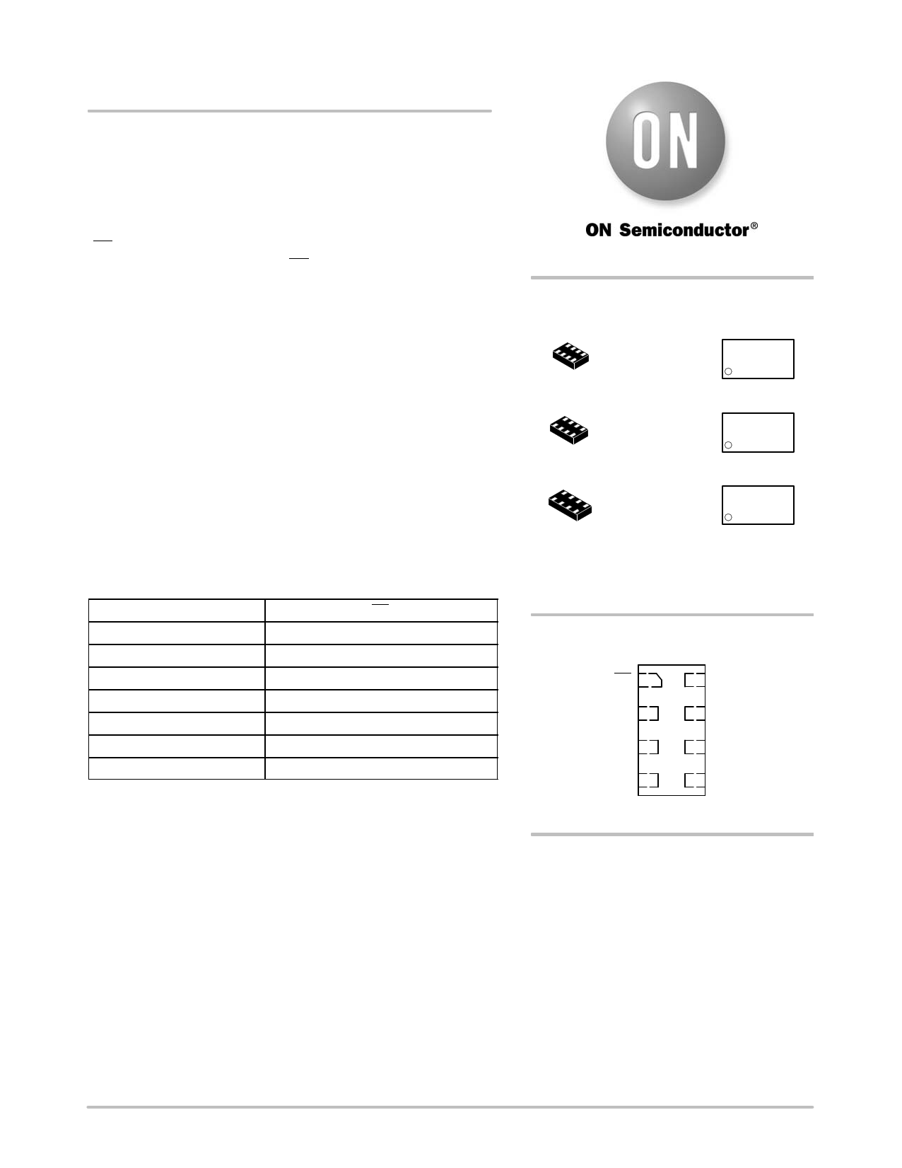
PIN ASSIGNMENT
1
2
3
4
5
6
7
8
OE
A
B
GND
C
D
Y
VCC
http://onsemi.com
MARKING
DIAGRAMS
ULLGA8
1.45 x 1.0
EM
1 CASE 613AA
1
ULLGA8
1.6 x 1.0
CASE 613AB
AAM
G
1
ULLGA8
1.95 x 1.0
CASE 613AC
AAM
G
AA or E = Specific Device Code
M = Date Code
G = Pb−Free Package
PIN ASSIGNMENTS
OE 1
A2
8 VCC
7Y
B3
6D
GND 4
5C
(Top View)
ORDERING INFORMATION
See detailed ordering and shipping information in the package
dimensions section on page 12 of this data sheet.
© Semiconductor Components Industries, LLC, 2008
September, 2008 − Rev. 0
www.DataSheet.in
1
Publication Order Number:
NLX1G99/D
1 page 
3−State NAND/OR Function Available
OE
Input 1
Input 2
NLX1G99
OE
Y Input 1
Input 2
Figure 9.
Y
No. of Inputs
2
2
AND/NAND Function
3−State NAND
3−State NAND
OR/NOR Function
3−State OR
3−State OR
OE
L
OE
Input 1
Input 2
OE
Y Input 1
Input 2
Figure 10.
A
L
L
B
Input 1
Input 2
C
Input 2
Input 1
Y
D
H
H
No. of Inputs
2
2
AND/NAND Function
3−State NAND
3−State NAND
OR/NOR Function
3−State OR
3−State OR
OE
L
A
Input 2
H
OE
Input 1
Input 2
OE
Y Input 1
Input 2
Figure 11.
B
L
Input 1
C
Input 1
Input 2
Y
D
H
L
No. of Inputs
2
2
AND/NAND Function
3−State NAND
3−State NAND
OR/NOR Function
3−State OR
3−State OR
OE
L
A
Input 1
H
OE
Input 1
Input 2
OE
Y Input 1
Input 2
Figure 12.
B
L
Input 2
C
Input 2
Input 1
Y
D
H
L
No. of Inputs
2
2
AND/NAND Function
3−State AND
3−State AND
OR/NOR Function
3−State OR
3−State OR
OE
L
ABCD
Input 1 H Input 2 L
Input 2 H Input 1 L
www.DataSheet.in
http://onsemi.com
5
5 Page 
From Output
Under Test
CL* RL
NLX1G99
RL S1 VLOAD
Open
GND
Test
tPLH/tPHL
tPLZ/tPZL
tPHZ/tPZH
S1
Open
VLOAD
GND
*CL includes probes and jig capacitance.
Figure 22. Load Circuit
VCC
1.8 V $ 0.15 V
2.5 V $ 0.2 V
3.3 V $ 0.3 V
5.5 V $ 0.5 V
Inputs
VI tr/tf
VCC v 2 ns
VCC v 2 ns
3 V v 2.5 ns
VCC v 2.5 ns
VM
VCC/2
VCC/2
1.5 V
VCC/2
VLOAD
2 x VCC
2 x VCC
6V
2 x VCC
CL
30 pF
30 pF
50 pF
50 pF
RL
1 kW
500 W
500 W
500 W
VD
0.15 V
0.15 V
0.3 V
0.3 V
Input
tW
VM
VI
VM
0V
Timing Input
Data Input
VM
tsu th
VM
VI
0V
VM VI
0V
Figure 23. Voltage Waveforms Pulse Duration
Input
tPLH
Output
tPHL
Output
VM
VM
VM
VI
VM 0 V
tPHL
VM
VOH
VOL
tPLH
VM
VOH
VOL
Figure 25. Voltage Waveforms Propagation Delay
Times Inverting and Noninverting Outputs
Figure 24. Voltage Waveforms Setup and Hold
Times
Output
Control
VM VM VI
0V
Output
Waveform 1
S1 at VLOAD
(Note 11)
tPZH
Output
Waveform 2
S1 at GND
(Note 11)
VM
VLOAD/2
VOL + VDVOL
tPHZ
VM
VOH − VVDOH
[0 V
Figure 26. Voltage Waveforms Enable and
Disable Times Low− and High−Level Enabling
11. Waveform 1 is for an output with internal conditions such that the output is low, except when disabled by the output control.
Waveform 2 is for an output with internal conditions such that the output is high, except when disabled by the output control
12. All input pulses are supplied by generators having the following characteristics: PRR v 10 MHz, ZO = 50 W.
13. The outputs are measured one at a time, with one transition per measurement.
14. All parameters are waveforms are not applicable to all devices.
www.DataSheet.in
http://onsemi.com
11
11 Page | ||
| Páginas | Total 15 Páginas | |
| PDF Descargar | [ Datasheet NLX1G99.PDF ] | |
Hoja de datos destacado
| Número de pieza | Descripción | Fabricantes |
| NLX1G97 | Configurable Multifunction Gate | ON Semiconductor |
| NLX1G98 | Configurable Multifunction Gate | ON Semiconductor |
| NLX1G99 | Configurable Multifunction Gate | ON Semiconductor |
| Número de pieza | Descripción | Fabricantes |
| SLA6805M | High Voltage 3 phase Motor Driver IC. |
Sanken |
| SDC1742 | 12- and 14-Bit Hybrid Synchro / Resolver-to-Digital Converters. |
Analog Devices |
|
DataSheet.es es una pagina web que funciona como un repositorio de manuales o hoja de datos de muchos de los productos más populares, |
| DataSheet.es | 2020 | Privacy Policy | Contacto | Buscar |