|
|
|
PDF NCV8668 Data sheet ( Hoja de datos )
| Número de pieza | NCV8668 | |
| Descripción | Very Low I 150 mA LDO Regulator | |
| Fabricantes | ON Semiconductor | |
| Logotipo | ||
Hay una vista previa y un enlace de descarga de NCV8668 (archivo pdf) en la parte inferior de esta página. Total 18 Páginas | ||
|
No Preview Available !
NCV8668
Very Low Iq 150 mA LDO
Regulator with Window
Watchdog, Enable and
Reset
The NCV8668 is 150 mA LDO regulator with integrated window
watchdog and reset functions dedicated for microprocessor
applications. Its robustness allows NCV8668 to be used in severe
automotive environments. Very low quiescent current as low as 38 mA
typical makes it suitable for applications permanently connected to
battery requiring very low quiescent current with or without load. The
Enable function can be used for further decrease of quiescent current
down to 1 mA.
The NCV8668 contains protection functions as current limit and
thermal shutdown.
Features
• Output Voltage Options: 3.3 V and 5 V
• Output Voltage Accuracy: $1.5% (TJ = 25°C to 125°C)
• Output Current up to 150 mA
• Very Low Quiescent Current: Typ 38 mA (max 43 mA)
• Very Low Dropout Voltage
• Enable Function
• Microprocessor Compatible Control Functions:
♦ Reset with Adjustable Power−on Delay
♦ Window Watchdog
• Wide Input Voltage Operation Range: up to 40 V
• Protection Features:
♦ Current Limitation
♦ Reverse Output Current
♦ Thermal Shutdown
• These are Pb−Free Devices
Typical Applications
• Body Control Module
• Instruments and Clusters
• Occupant Protection and Comfort
• Powertrain
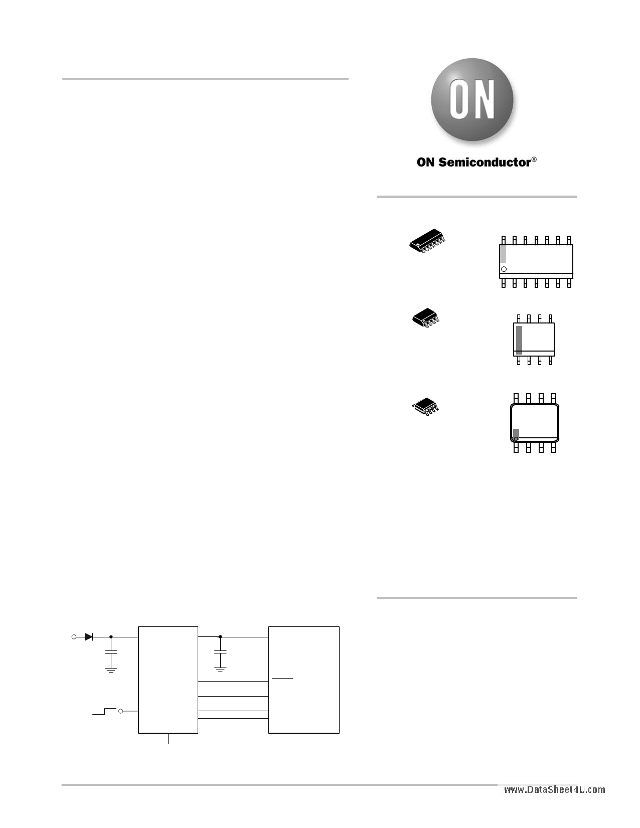
VBAT
Vout
V in V out
Cin
0.1 mF
NCV8668
Cout
2.2 mF
OFF ON
RO
WDI
EN WM1
WM2
GND
VDD
Microprocessor
RESET
I/O
I/O
I/O
Figure 1. Application Schematic
www.DataSheet4U.com
http://onsemi.com
14
1
SOIC−14
CASE 751A
MARKING
DIAGRAMS
14
V8668ZZXXG
AWLYWW
1
8
1
SOIC−8
D SUFFIX
CASE 751A
8
668ZZX
ALYW
G
1
8
1
SOIC−8 EP
CASE 751AC
8
668ZZX
AYWWG
G
1
ZZ = Timing, Reset Threshold,
Watchdog Control Options*
XX,X = Voltage Options
= 5 V (XX = 50, X = 5)
= 3.3 V (XX = 33, X = 3)
A = Assembly Location
WL, L = Wafer Lot
YY, Y = Year
WW, W = Work Week
G or G = Pb−Free Package
*See APPLICATION INFORMATION Section.
ORDERING INFORMATION
See detailed ordering and shipping information in the package
dimensions section on page 15 of this data sheet.
© Semiconductor Components Industries, LLC, 2010
October, 2010 − Rev. 2
1
Publication Order Number:
NCV8668/D
1 page 
NCV8668
ELECTRICAL CHARACTERISTICS
Vin = 13.2 V, Cin = 0.1 mF, Cout = 2.2 mF, for typical values TJ = 25°C, for min/max values TJ = −40°C to 150°C; unless otherwise noted.
(Notes 10 and 11)
www.DataSheet4U.com
Parameter
Test Conditions
Symbol Min Typ Max Unit
Disable and Quiescent Current
Disable Current
Quiescent Current (Iq = Iin – Iout)
Current Limit Protection
VEN = 0 V,TJ < 85°C
Iout = 100 mA, TJ = 25°C
Iout = 100 mA, TJ v 125°C
IDIS − − 1 mA
Iq mA
− 38 43
− − 44
Current Limit
Short Circuit Current Limit
Reverse Output Current Protection
Vout = 0.96 x Vout_nom
Vout = 0 V
ILIM 205 − 525 mA
ISC 205 − 525 mA
Reverse Output Current Protection
PSRR
VEN = 0 V, Iout = −1 mA
Vout_rev
−
2 5.5 V
Power Supply Ripple Rejection (Note 13) f = 100 Hz, 0.5Vpp
Enable Thresholds
PSRR
− 60 − dB
Enable Input Threshold Voltage
Logic High
Logic Low
Vth(EN)
V
3−−
− − 0.8
Enable Input Current
Logic High
Logic Low
Window Watchdog
VEN = 5 V
VEN = 0 V, TJ < 85°C
mA
IEN_ON − 3 5
IEN_OFF − 0.5 1
Watchdog Mode Bit 1 Threshold Voltage
Voltage Increasing, Logic High
3.3 V
5.0 V
Voltage Decreasing, Logic Low
Watchdog Mode Bit 2 Threshold Voltage
Voltage Increasing, Logic High
3.3 V
5.0 V
Voltage Decreasing, Logic Low
Watchdog Input WDI Threshold Voltage
Voltage Increasing, Logic High
3.3 V
5.0 V
Voltage Decreasing, Logic Low
Watchdog Input WDI Current
Logic High
Logic Low
Watchdog Sampling Time
VWDI,H = 5 V
VWDI,L = 0 V, TJ < 85 °C
Fast:
Slow:
WM2 = L
WM1 = L AND WM2 = H
VWM1,H
VWM1,L
−
−
0.8
V
− 2.65
− 4.0
−−
VWM2,H
VWM2,L
−
−
0.8
V
− 2.65
− 4.0
−−
V
VWDI,H
− − 2.65
− − 4.0
VWDI,L 0.8 −
−
IWDI,H
IWDI,L
mA
−34
− 0.5 1
tsam 0.4 0.5 0.6 ms
0.8 1.0 1.2
Ignore Window Time
Fast:
Slow:
WM2 = L
WM1 = L AND WM2 = H
tIW 25.6 32.0 38.4 ms
51.2 64.0 76.8
Open Window Time
Fast:
Slow:
WM2 = L
WM1 = L AND WM2 = H
tOW
25.6 32.0 38.4
51.2 64.0 76.8
ms
Closed Window Time
Fast:
Slow:
WM2 = L
WM1 = L AND WM2 = H
tCW 25.6 32.0 38.4 ms
51.2 64.0 76.8
10. Refer to ABSOLUTE MAXIMUM RATINGS and APPLICATION INFORMATION for Safe Operating Area.
11. Performance guaranteed over the indicated operating temperature range by design and/or characterization tested at TA [TJ. Low duty
cycle pulse techniques are used during testing to maintain the junction temperature as close to ambient as possible.
12. Measured when output voltage falls 100 mV below the regulated voltage at Vin = 13.2 V. If Vout < 5 V, then VDO = Vin – Vout. Maximum dro-
pout voltage value is limited by minimum input voltage Vin = 4.5 V recommended for guaranteed operation at maximum output current.
13. Values based on design and/or characterization.
14. Recommended for typical trigger time. TWD = tCW + 1/2 * tOW
http://onsemi.com
5
5 Page 
NCV8668
TYPICAL CHARACTERISTICS
Vin
www.DataSheet4U.com
Vout
VRT+ VRhys
VRT
VRO
VROH
VROL
< tRR
tRD
tRR
Figure 24. Reset Function and Timing Diagram
Trigger
Reset &
Disabled
Watchdog
Reset
Trigger
No Trigger
WD_ON
WD_ON
Long
Open
Window
Ignore
Window
WD_OFF or
Iout < Iout_WD_OFF
WD_OFF or
Iout < Iout_WD_OFF
No Trigger
Trigger
t
t
t
Disabled
Watchdog
WD_OFF or
Iout < Iout_WD_OFF
WD_OFF or
Iout < Iout_WD_OFF
Open
Window
No Trigger
Trigger
Closed
Window
WM1
WM2
Window Watchdog Mode
Reset Mode
L
L
FAST
FAST
L
H
SLOW
SLOW
H
L
FAST
SLOW
H
H
OFF
SLOW
Figure 25. Window Watchdog State Diagram, Watchdog and Reset Modes
http://onsemi.com
11
11 Page | ||
| Páginas | Total 18 Páginas | |
| PDF Descargar | [ Datasheet NCV8668.PDF ] | |
Hoja de datos destacado
| Número de pieza | Descripción | Fabricantes |
| NCV8660 | Very Low Iq LD0 150 mA Regulator | ON Semiconductor |
| NCV8660B | LD0 150 mA Regulator | ON Semiconductor |
| NCV8664 | Ultra Low Dropout Linear Regulator | ON Semiconductor |
| NCV8664C | Low Dropout Linear Regulator | ON Semiconductor |
| Número de pieza | Descripción | Fabricantes |
| SLA6805M | High Voltage 3 phase Motor Driver IC. |
Sanken |
| SDC1742 | 12- and 14-Bit Hybrid Synchro / Resolver-to-Digital Converters. |
Analog Devices |
|
DataSheet.es es una pagina web que funciona como un repositorio de manuales o hoja de datos de muchos de los productos más populares, |
| DataSheet.es | 2020 | Privacy Policy | Contacto | Buscar |