|
|
|
PDF ADXRS649 Data sheet ( Hoja de datos )
| Número de pieza | ADXRS649 | |
| Descripción | Vibration Rejecting Rate Gyro | |
| Fabricantes | Analog Devices | |
| Logotipo | ||
Hay una vista previa y un enlace de descarga de ADXRS649 (archivo pdf) en la parte inferior de esta página. Total 12 Páginas | ||
|
No Preview Available !
FEATURES
High vibration rejection over wide frequency
Ultrafast startup: 3 ms
Measurement range extendable to ±50,000°/sec
10,000 g powered shock survivability
Ratiometric to referenced supply
5 V single-supply operation
Z-axis (yaw rate) response
−40°C to +105°C operation
Self-test on digital command
Ultrasmall and light (<0.15 cc, <0.5 gram)
Temperature sensor output
RoHS compliant
APPLICATIONS
Sports equipment
Industrial applications
Platform stabilization
High speed tachometry
Fast Starting, ±20,000°/sec
Vibration Rejecting Rate Gyro
ADXRS649
GENERAL DESCRIPTION
The ADXRS649 is a complete angular rate sensor (gyroscope)
that uses the Analog Devices, Inc., patented high volume BiMOS
surface-micromachining process to make a complete gyro on
one chip. An advanced, differential, quad sensor design rejects
the influence of linear acceleration, enabling the ADXRS649
to offer rate sensing in harsh environments where shock and
vibration are present.
The output signal, RATEOUT (B1, A2), is a voltage proportional
to the angular rate about the axis normal to the top surface of
the package. The output is ratiometric with respect to a provided
reference supply. An external capacitor is used to set the band-
width. The measurement range is extendable to ±50,000°/sec
by adding an external resistor.
Low power consumption (3.5 mA) enables very low power
consumption, and ultrafast startup (3 ms) allows for quick
power cycling of the gyro. At 10 samples per second, a pair of
CR2032 coin cells can power the ADXRS649 for three months.
A temperature output is provided for compensation techniques.
Two digital self-test inputs electromechanically excite the sensor
to test proper operation of both the sensor and the signal condi-
tioning circuits. The ADXRS649 is available in a 7 mm × 7 mm ×
3 mm CBGA chip scale package.
www.DataSheet4U.com
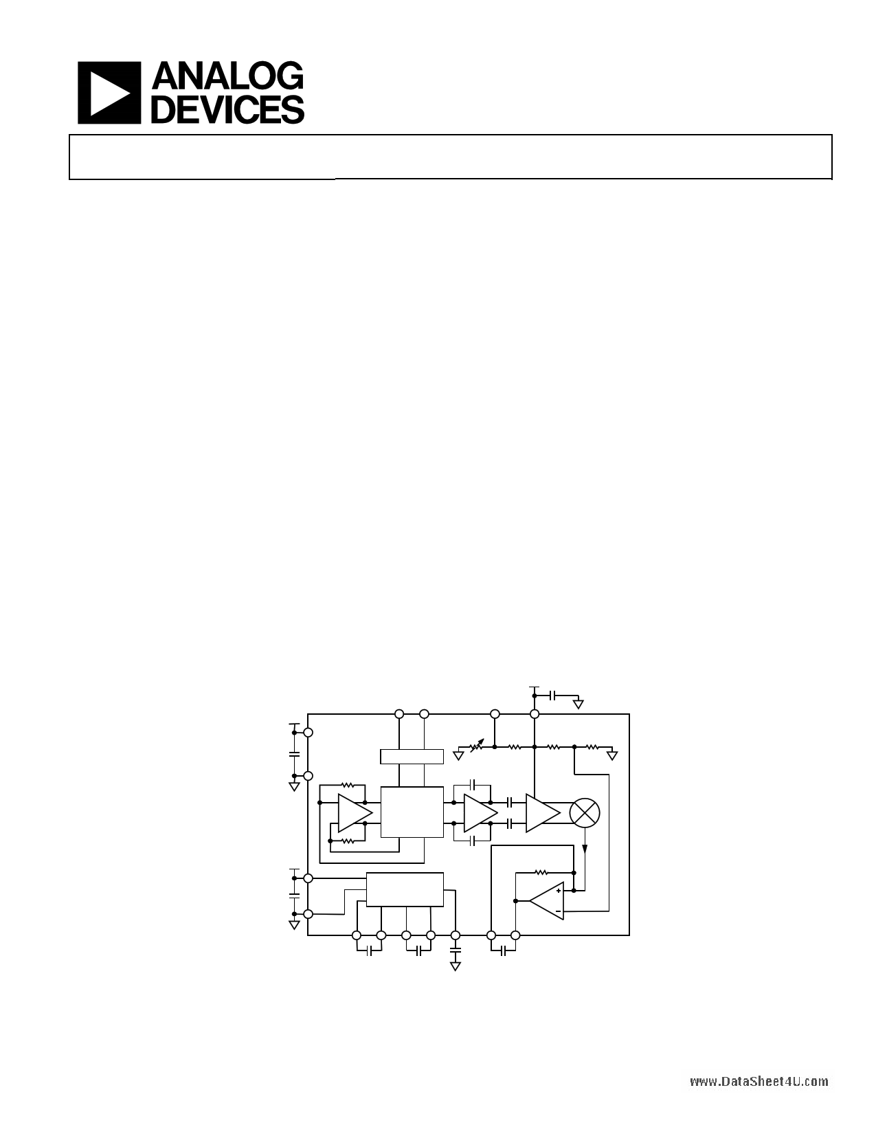
FUNCTIONAL BLOCK DIAGRAM
5V
(ADC REF)
100nF
5V
100nF
AVCC
AGND
ST2 ST1
SELF-TEST
DRIVE
AMP
MECHANICAL
SENSOR
TEMP VRATIO
ADXRS649
25kΩ 25kΩ
AT 25°C
AC
AMP
VGA
DEMOD
5V
VDD
100nF
PGND
CHARGE PUMP
AND VOLTAGE
REGULATOR
CP1 CP2 CP3 CP4 CP5 SUMJ
ROUT
180kΩ ±1%
RATEOUT
22nF
22nF
2.2nF
COUT
Figure 1.
Rev. 0
Information furnished by Analog Devices is believed to be accurate and reliable. However, no
responsibility is assumed by Analog Devices for its use, nor for any infringements of patents or other
rights of third parties that may result from its use. Specifications subject to change without notice. No
license is granted by implication or otherwise under any patent or patent rights of Analog Devices.
Trademarksandregisteredtrademarksarethepropertyoftheirrespectiveowners.
One Technology Way, P.O. Box 9106, Norwood, MA 02062-9106, U.S.A.
Tel: 781.329.4700
www.analog.com
Fax: 781.461.3113
©2010 Analog Devices, Inc. All rights reserved.
1 page 
PIN CONFIGURATION AND FUNCTION DESCRIPTIONS
PGND
VDD CP5 CP3
CP4
7
ST1
ST2
TEMP
6
CP1
5
CP2
4
AVCC 3
2
Table 3. Pin Function Descriptions
Pin No.
Mnemonic
D6, D7
CP5
A6, B7
CP4
C6, C7
CP3
A5, B5
CP1
A4, B4
CP2
A3, B3
AVCC
B1, A2
RATEOUT
C1, C2
SUMJ
D1, D2
NC
E1, E2
VRATIO
F1, G2
AGND
F3, G3
TEMP
F4, G4
ST2
F5, G5
ST1
G6, F7
PGND
E6, E7
VDD
AGND
VRATIO NC SUMJ
GF E D C BA
NOTES
1. NC = NO CONNECT. DO NOT CONNECT TO THIS PIN.
Figure 3. Pin Configuration
1
RATEOUT
Description
High Voltage Filter Capacitor, 2.2 nF.
Charge Pump Capacitor, 22 nF.
Charge Pump Capacitor, 22 nF.
Charge Pump Capacitor, 22 nF.
Charge Pump Capacitor, 22 nF.
Positive Analog Supply.
Rate Signal Output.
Output Amplifier Summing Junction.
Do not connect to these pins.
Reference Supply for Ratiometric Output.
Analog Supply Return.
Temperature Voltage Output.
Self-Test for Sensor 2.
Self-Test for Sensor 1.
Charge Pump Supply Return.
Positive Charge Pump Supply.
ADXRS649
www.DataSheet4U.com
Rev. 0 | Page 5 of 12
5 Page 
OUTLINE DIMENSIONS
ADXRS649
A1 BALL
CORNER
3.80 MAX
7.05
6.85 SQ
6.70
TOP VIEW
DETAIL A
4.80
BSC SQ
0.80
BSC
7654321
BOTTOM VIEW
*A1 CORNER
INDEX AREA
A
B
C
D
E
F
G
0.60 MAX
0.25 MIN
SEATING
PLANE
DETAIL A
0.60
0.55
0.50
3.20 MAX
2.50 MIN
COPLANARITY
0.15
BALL DIAMETER
*BALL A1 IDENTIFIER IS GOLD PLATED AND CONNECTED
TO THE D/A PAD INTERNALLY VIA HOLES.
Figure 20. 32-Lead Ceramic Ball Grid Array [CBGA]
(BG-32-3)
Dimensions shown in millimeters
ORDERING GUIDE
Model1
ADXRS649BBGZ-RL
EVAL-ADXRS649Z
1 Z = RoHS Compliant Part.
Temperature Range
–40°C to +105°C
Package Description
32-Lead Ceramic Ball Grid Array [CBGA]
Evaluation Board
Package Option
BG-32-3
www.DataSheet4U.com
Rev. 0 | Page 11 of 12
11 Page | ||
| Páginas | Total 12 Páginas | |
| PDF Descargar | [ Datasheet ADXRS649.PDF ] | |
Hoja de datos destacado
| Número de pieza | Descripción | Fabricantes |
| ADXRS642 | Vibration Rejecting Yaw Rate Gyro | Analog Devices |
| ADXRS645 | Gyroscope | Analog Devices |
| ADXRS646 | Low Noise Vibration Rejecting Yaw Rate Gyro | Analog Devices |
| ADXRS649 | Vibration Rejecting Rate Gyro | Analog Devices |
| Número de pieza | Descripción | Fabricantes |
| SLA6805M | High Voltage 3 phase Motor Driver IC. |
Sanken |
| SDC1742 | 12- and 14-Bit Hybrid Synchro / Resolver-to-Digital Converters. |
Analog Devices |
|
DataSheet.es es una pagina web que funciona como un repositorio de manuales o hoja de datos de muchos de los productos más populares, |
| DataSheet.es | 2020 | Privacy Policy | Contacto | Buscar |