|
|
|
PDF L11815B Data sheet ( Hoja de datos )
| Número de pieza | L11815B | |
| Descripción | 1.5A CMOS LDO | |
| Fabricantes | Unisonic Technologies | |
| Logotipo | ||
Hay una vista previa y un enlace de descarga de L11815B (archivo pdf) en la parte inferior de esta página. Total 6 Páginas | ||
|
No Preview Available !
UNISONIC TECHNOLOGIES CO., LTD
L11815B
Preliminary
1.5A CMOS LDO
DESCRIPTION
The UTC L11815B is a positive, linear regulator. One of its
features is the very low quiescent current typically as low as 45μA
and the dropout voltage is extremely low.
The internal circuit includes thermal shutdown and current
fold-back mechanism to prevent device failure when the circuit is
operated in the bad conditions.
In application, the UTC L11815B needs a low noise and
regulated supply. For stability, the output capacitance value should
be 4.7μF or more.
The UTC L11815B is an ideal for battery applications, such as
instrumentations, portable electronics, wireless devices, cordless
phones, PC peripherals, and battery powered widgets. The output
voltage values are set during manufacturing and their accuracy is
trimmed to within 1.5%.
FEATURES
* Quiescent Current (45μA typ.)
* Accurate :±1.5%
* Very Low Dropout Voltage
* Guaranteed 1.5A Output
* Over-Temperature Shutdown
* With Current Limiting
* Short Circuit Current Fold-Back
* Power-Saving Shutdown Mode
* Low Temperature Coefficient
* Halogen Free
ORDERING INFORMATION
Ordering Number
Package
Packing
L11815BG-xx-x-S08-R
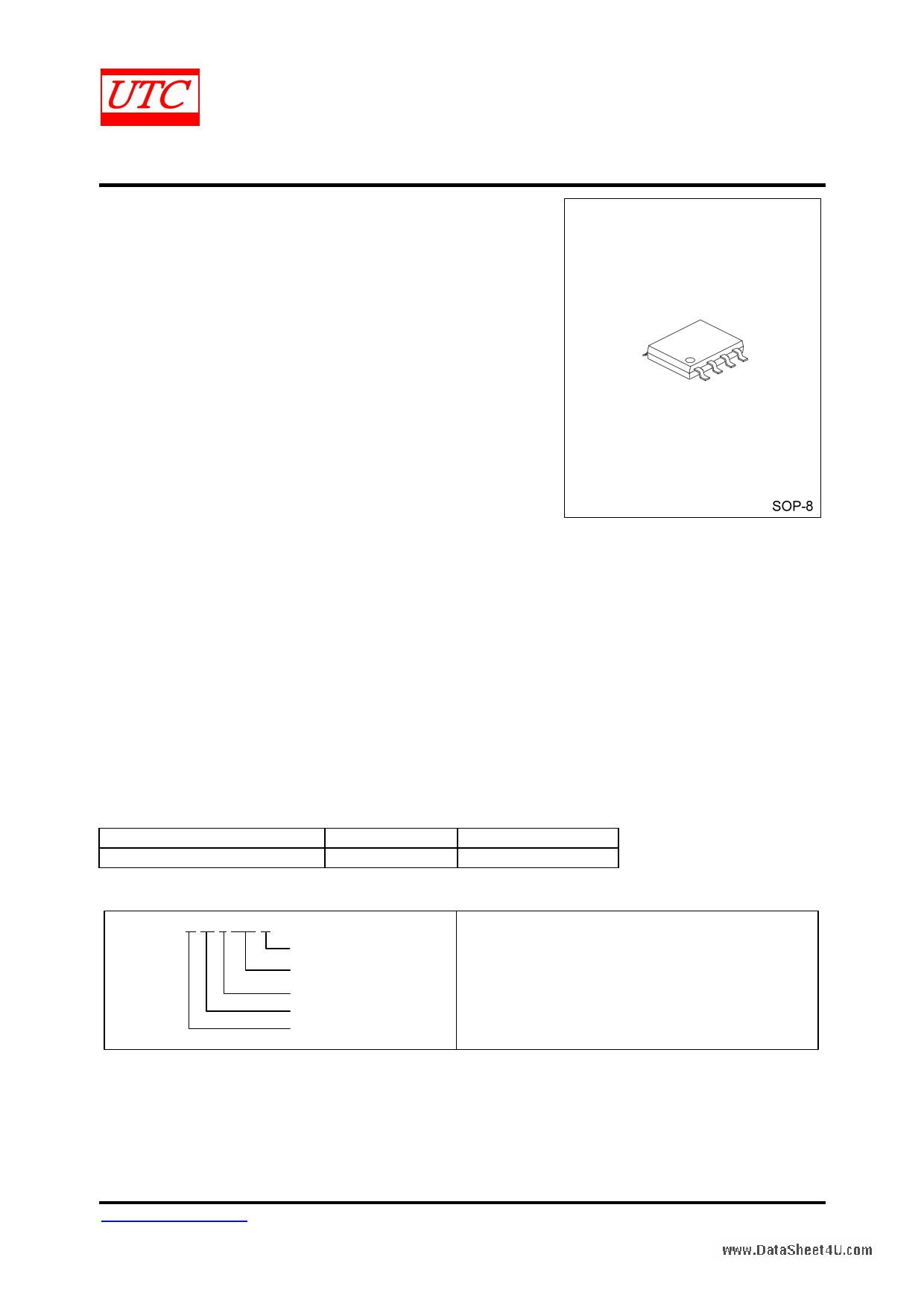
SOP-8
Tape Reel
Note: xx: Output Voltage, x: Pin Code; refer to Marking Information.
L11815BG-xx-x-S08-R
(1) Packing Type
(2) Package Type
(3) Pin Code
(4) Output Voltage Code
(5) Halogen Free
(1) R: Tape Reel
(2) S08: SOP-8
(3) x: Pin Code
(4) xx: Refer to Marking Information
(5) G: Halogen Free
www.DataSheet4U.com
CMOS IC
www.unisonic.com.tw
Copyright © 2010 Unisonic Technologies Co., Ltd
1 of 6
QW-R502-352.c
1 page 
L11815B
Preliminary
CMOS IC
DETAILED DESCRIPTION
The UTC L11815B of CMOS regulators insist of a PMOS pass transistor, voltage reference, error amplifier,
over-current protection, and thermal shutdown.
The error amplifier, over-current shutdown, and thermal protection circuits provides data for P-channel pass
transistor. The error amplifier takes output voltage for a precision reference in the normal operation and the normal
operation is restored when the junction temperature drops below 120°C. Over-current and Thermal shutdown circuits
start to work when the junction temperature is higher than 140°C, or the current is higher than 2.2A. The output
voltage stays low when the thermal shutdown is in active.
The UTC L11815B behaves like a current source when the load reaches 2.2A. But the current would fall back to
600mA to prevent excessive power loss when the load impedance value is below 0.3Ω.Normal operation is restored
when the load resistance value is higher than 0.75 Ω.
EXTERNAL CAPACITORS
The UTC L11815B has an output capacitor to ground of 4.7μF or more in the stable operation. Ceramic
capacitors can provide the lowest ESR with the best AC performance. Aluminum Electrolytic capacitors, in contrast,
have the highest ESR with poorest AC response. Unfortunately, large value ceramic capacitors are comparatively
expensive. So we can parallel a 0.1μF ceramic capacitor with a 10μF Aluminum Electrolytic. The result is low ESR,
high capacitance, and low overall cost.
A second capacitor is recommended between the input and ground to stabilize input voltage. To get an ideal
effect the value of the input capacitor should be at least 0.1μF.
A third capacitor can be connected between the bypass pin and ground. This capacitor can be a low cost
Polyester Film varies in the range of 0.001 ~ 0.01μF. A larger capacitor improves the AC ripple rejection, but also
makes the output come up slowly. This "Soft" turn-on is desirable in some applications to limit turn-on surges.
At last, all the capacitors should keep a close proximity to the pins; you can achieve this with a star connection.
ENABLE
When pulled low, the PMOS pass transistor shuts off, and all internal circuits are powered down. In this state, the
quiescent current is less than 1μA. This pin behaves much like an electronic switch.
100kΩ resistor is necessary between VEN source and EN pin when VEN is higher than VIN.
(Note: There is no internal pull-up for EN PIN.)
ADJUSTABLE VERSION
The adjustable version uses external feedback resistors to generate an output voltage anywhere from 1.5V to
5.0V. VADJ is trimmed to 1.2V and VOUT is given by the equation:
VOUT = VADJ (1 + R1 / R2)
Feedback resistors R1 and R2 should be high enough to keep quiescent current low, but increasing R1 + R2 will
reduce stability. In general, R1 and R2 in the 10’s of kΩ will produce adequate stability, given reasonable layout
precautions. To improve stability characteristics, keep parasitics on the ADJ pin to a minimum, and lower R1 and R2
values.
www.DataSheet4U.com
UNISONIC TECHNOLOGIES CO., LTD
www.unisonic.com.tw
5 of 6
QW-R502-352.c
5 Page | ||
| Páginas | Total 6 Páginas | |
| PDF Descargar | [ Datasheet L11815B.PDF ] | |
Hoja de datos destacado
| Número de pieza | Descripción | Fabricantes |
| L11815A | 1.5A CMOS LDO | Unisonic Technologies |
| L11815B | 1.5A CMOS LDO | Unisonic Technologies |
| Número de pieza | Descripción | Fabricantes |
| SLA6805M | High Voltage 3 phase Motor Driver IC. |
Sanken |
| SDC1742 | 12- and 14-Bit Hybrid Synchro / Resolver-to-Digital Converters. |
Analog Devices |
|
DataSheet.es es una pagina web que funciona como un repositorio de manuales o hoja de datos de muchos de los productos más populares, |
| DataSheet.es | 2020 | Privacy Policy | Contacto | Buscar |