|
|
|
PDF AD7280A Data sheet ( Hoja de datos )
| Número de pieza | AD7280A | |
| Descripción | Lithium Ion Battery Monitoring System Cell balancing interface | |
| Fabricantes | Analog Devices | |
| Logotipo | ||
Hay una vista previa y un enlace de descarga de AD7280A (archivo pdf) en la parte inferior de esta página. Total 30 Páginas | ||
|
No Preview Available !
www.DataSheet4U.net
Lithium Ion Battery Monitoring System
AD7280A
FEATURES
12-bit ADC, 1 μs per channel conversion time
6 analog input channels, common-mode
range 0.5 V to 27.5 V
6 auxiliary ADC inputs
±1.6 mV cell voltage accuracy
On-chip voltage regulator
Cell balancing interface
Daisy-chain interface
Internal reference: ±3 ppm/oC
1.8 μA power-down current
High input impedance
Serial interface with alert function
1 SPI interface for up to 48 channels
CRC protection on read and write commands
On-chip registers for channel sequencing
VDD operating range: 8 V to 30 V
Temperature range: −40°C to +105°C
48-lead LQFP
Qualified for automotive applications
APPLICATIONS
Lithium ion battery monitoring
Electric and hybrid electric vehicles
Power supply backup
Power tools
GENERAL DESCRIPTION
The AD7280A1 contains all the functions required for general-
purpose monitoring of stacked lithium ion batteries as used in
hybrid electric vehicles, battery backup applications, and power
tools. The part has multiplexed cell voltage and auxiliary ADC
measurement channels for up to six cells of battery management.
An internal ±3 ppm/°C reference is provided that allows a cell
voltage accuracy of ±1.6 mV. The ADC resolution is 12 bits and
allows conversion of up to 48 cells within 7 μs.
The AD7280A operates from a single VDD supply that has a
range of 8 V to 30 V (with an absolute maximum rating of
33 V). The part provides six differential analog input channels
to accommodate large common-mode signals across the full
VDD range. Each channel allows an input signal range, VIN(+)
− VIN(−), of 1 V to 5 V. The input pins assume a series stack of
six cells. In addition, the part includes six auxiliary ADC input
channels that can be used for temperature measurement or
system diagnostics.
1 Patents pending.
Rev. 0
Information furnished by Analog Devices is believed to be accurate and reliable. However, no
responsibility is assumed by Analog Devices for its use, nor for any infringements of patents or other
rights of third parties that may result from its use. Specifications subject to change without notice. No
license is granted by implication or otherwise under any patent or patent rights of Analog Devices.
Trademarksandregisteredtrademarksarethepropertyoftheirrespectiveowners.
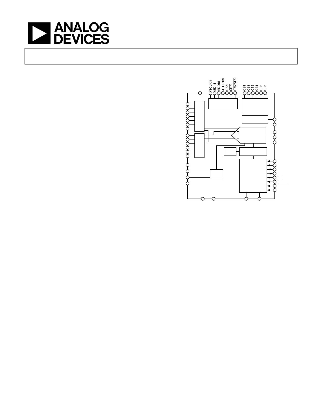
FUNCTIONAL BLOCK DIAGRAM
VIN6
VIN5
VIN4
VIN3
VIN2
VIN1
VIN0
AUX6
AUX5
AUX4
AUX3
AUX2
AUX1
AUXTERM
VREF
CREF
REFGND
VDD
HV
MUX
DAISY-CHAIN
INTERFACE
AD7280A
CELL
BALANCING
INTERFACE
REGULATOR
LV
MUX
12-BIT ADC
CLOCK
CONTROL LOGIC
AND SELF-TEST
2.5V
REF
LIMIT REG
SQN LOGIC
DATA MEMORY
SPI INTERFACE
VSS AGND
SDOlo ALERTlo
Figure 1.
VREG
DGND
DVCC
AVCC
VDRIVE
SCLK
SDI
SDO
ALERT
CS
PD
CNVST
MASTER
The AD7280A includes on-chip registers that allow a sequence
of channel measurements to be programmed to suit the application
requirements.
The AD7280A also includes a dynamic alert function that can
detect whether the cell voltages or auxiliary ADC inputs exceed
an upper or lower limit defined by the user. The AD7280A has
cell balancing interface outputs designed to control external FET
transistors to allow discharging of individual cells.
The AD7280A includes a built-in self-test feature that internally
applies a known voltage to the ADC inputs.
A daisy-chain interface allows up to eight parts to be stacked
without the need for individual device isolation.
The AD7280A requires only one supply pin that accepts 6.9 mA
under normal operation while converting at 1 MSPS.
All this functionality is provided in a 48-lead LQFP package
operating over a temperature range of −40°C to +105°C.
One Technology Way, P.O. Box 9106, Norwood, MA 02062-9106, U.S.A.
Tel: 781.329.4700
www.analog.com
Fax: 781.461.3113
©2011 Analog Devices, Inc. All rights reserved.
1 page 
AD7280A
POWER SPECIFICATIONS
VDD = 8 V to 30 V, VSS = 0 V, DVCC = AVCC = VREG, VDRIVE = 2.7 V to 5.5 V, TA = −40°C to +105°C, unless otherwise noted.
Table 2.
Parameter
POWER REQUIREMENTS
VDD
Master Device
IDD During Conversion
IDD During Data Readback
IDD During Cell Balancing
IDD Software Power-Down
IDD Full Power-Down Mode
Slave Device
IDD During Conversion
IDD During Data Readback
IDD During Cell Balancing
IDD Software Power-Down
IDD Full Power-Down Mode
POWER DISSIPATION
Master Device
During Conversion
During Data Readback
During Cell Balancing
Software Power-Down
Full Power-Down Mode
Slave Device
During Conversion
During Data Readback
During Cell Balancing
Software Power-Down
Full Power-Down Mode
Min Typ Max Unit Test Conditions/Comments
8 30 V
5.6 7.3 mA
5.3 7.0 mA
5.1 6.8 mA
2.5 2.9 mA
1.8 5
μA
6.9 8.7 mA
6.5 8.2 mA
6.4 8.0 mA
3.8 4.2 mA
1.8 5
μA
VDD = 30 V
170 220 mW
160 210 mW
155 205 mW
75 90 mW
54 150 μW
VDD = 30 V
210 265 mW
195 250 mW
192 240 mW
115 130 mW
54 150 μW
Rev. 0 | Page 5 of 48
5 Page 
TYPICAL PERFORMANCE CHARACTERISTICS
5.5
VDD = 8V
VDD = 10V
5.4
VDD = 22.5V
VDD = 29.9V
5.3
5.2
5.1
5.0
4.9
–40
–20
0 20 40 60
TEMPERATURE (°C)
80 100
Figure 4. VREG vs. Temperature for Different Supply Voltages,
VREG Connected to AVCC and DVCC
5.5
VDD = 8V
VDD = 10V
5.4
VDD = 22.5V
VDD = 29.9V
5.3
5.2
5.1
5.0
4.9
–40
–20
0 20 40 60
TEMPERATURE (°C)
80 100
Figure 5. VREG vs. Temperature for Different Supply Voltages,
VREG Connected to AVCC and DVCC, 5 mA External Load
8
SLAVE CURRENTS
7
6 MASTER CURRENTS
5
4
3
2
1
–40 –20
SLAVE, VDD = 8V
SLAVE, VDD = 10V
SLAVE, VDD = 29.9V
MASTER, VDD = 8V
MASTER, VDD = 10V
MASTER, VDD = 29.9V
0 20 40 60
TEMPERATURE (°C)
80 100
Figure 6. IDD During Conversion vs. Temperature
for Different Supply Voltages
AD7280A
8
7 SLAVE CURRENTS
6
MASTER CURRENTS
5
4
3
2
1
–40 –20
SLAVE, VDD = 8V
SLAVE, VDD = 10V
SLAVE, VDD = 29.9V
MASTER, VDD = 8V
MASTER, VDD = 10V
MASTER, VDD = 29.9V
0 20 40 60
TEMPERATURE (°C)
80 100
Figure 7. IDD During Cell Balancing vs. Temperature
for Different Supply Voltages
8
SLAVE, VDD = 8V
SLAVE, VDD = 10V
7 SLAVE, VDD = 29.9V
MASTER, VDD = 8V
6
MASTER, VDD = 10V
MASTER, VDD = 29.9V
5
4 SLAVE CURRENTS
3
MASTER CURRENTS
2
1
–40 –20
0 20 40 60
TEMPERATURE (°C)
80 100
Figure 8. IDD During Software Power-Down vs. Temperature
for Different Supply Voltages
10,000
8000
9149
6000
4000
2000
460
5
386
0
2660 2661 2662 2663 2664 2665 2666 2667 2668
CODE
Figure 9. Histogram of Codes for 10,000 Samples,
Odd Cell Voltage Channels
Rev. 0 | Page 11 of 48
11 Page | ||
| Páginas | Total 30 Páginas | |
| PDF Descargar | [ Datasheet AD7280A.PDF ] | |
Hoja de datos destacado
| Número de pieza | Descripción | Fabricantes |
| AD7280 | Lithium Ion Battery Monitoring System | Analog Devices |
| AD7280A | Lithium Ion Battery Monitoring System Cell balancing interface | Analog Devices |
| Número de pieza | Descripción | Fabricantes |
| SLA6805M | High Voltage 3 phase Motor Driver IC. |
Sanken |
| SDC1742 | 12- and 14-Bit Hybrid Synchro / Resolver-to-Digital Converters. |
Analog Devices |
|
DataSheet.es es una pagina web que funciona como un repositorio de manuales o hoja de datos de muchos de los productos más populares, |
| DataSheet.es | 2020 | Privacy Policy | Contacto | Buscar |