|
|
|
PDF NVTFS4823N Data sheet ( Hoja de datos )
| Número de pieza | NVTFS4823N | |
| Descripción | Power MOSFET ( Transistor ) | |
| Fabricantes | ON Semiconductor | |
| Logotipo | ||
Hay una vista previa y un enlace de descarga de NVTFS4823N (archivo pdf) en la parte inferior de esta página. Total 6 Páginas | ||
|
No Preview Available !
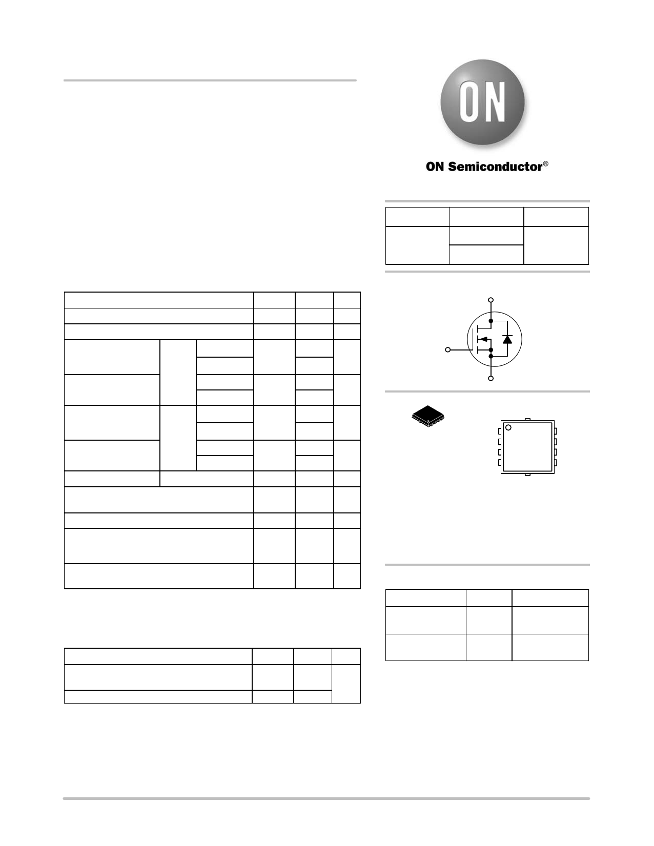
NVTFS4823N
Power MOSFET
30 V, 10.5 mW, 30 A, Single N−Channel
Features
• Small Footprint (3.3x3.3 mm) for Compact Design
• Low RDS(on) to Minimize Conduction Losses
• Low Capacitance to Minimize Driver Losses
• NV Prefix for Automotive and Other Applications Requiring
AEC−Q101 Qualified Site and Change Controls
• These are Pb−Free Devices
MAXIMUM RATINGS (TJ = 25°C unless otherwise noted)
Parameter
Symbol Value
Unit
Drain−to−Source Voltage
Gate−to−Source Voltage
Continuous Drain Cur-
r2e,n3t,R4Y) J−mb (Notes 1,
Power Dissipation
RYJ−mb (Notes 1, 2, 3)
Steady
State
Tmb = 25°C
Tmb = 100°C
Tmb = 25°C
Tmb = 100°C
Continuous Drain Cur-
rent
& 4)
RqJA
(Notes
1,
3,
Power Dissipation
RqJA (Notes 1, 3)
Steady
State
TA = 25°C
TA = 100°C
TA = 25°C
TA = 100°C
Pulsed Drain Current TA = 25°C, tp = 10 ms
Operating Junction and Storage Temperature
VDSS
VGS
ID
PD
ID
PD
IDM
TJ, Tstg
30
"20
30
21
21
11
13
9.0
3.1
1.6
198
−55 to
175
V
V
A
W
A
W
A
°C
Source Current (Body Diode)
Single Pulse Drain−to−Source Avalanche
Energy (TJ = 25°C, VDD = 24 V, VGS = 10 V,
IL(pk) = 24 A, L = 0.1 mH, RG = 25 W)
Lead Temperature for Soldering Purposes
(1/8″ from case for 10 s)
IS 19 A
EAS 28.8 mJ
TL 260 °C
Stresses exceeding Maximum Ratings may damage the device. Maximum
Ratings are stress ratings only. Functional operation above the Recommended
Operating Conditions is not implied. Extended exposure to stresses above the
Recommended Operating Conditions may affect device reliability.
THERMAL RESISTANCE MAXIMUM RATINGS (Note 1)
Parameter
Symbol Value Unit
Junction−to−Mounting Board (top) − Steady
State (Note 2, 3)
RYJ−mb
7.0 °C/W
Junction−to−Ambient − Steady State (Note 3)
RqJA
47
1. The entire application environment impacts the thermal resistance values shown,
they are not constants and are only valid for the particular conditions noted.
2. Psi (Y) is used as required per JESD51−12 for packages in which
substantially less than 100% of the heat flows to single case surface.
3. Surface−mounted on FR4 board using a 650 mm2, 2 oz. Cu pad.
4. Maximum current for pulses as long as 1 second is higher but is dependent
on pulse duration and duty cycle.
http://onsemi.com
V(BR)DSS
30 V
RDS(on) MAX
10.5 mW @ 10 V
17.5 mW @ 4.5 V
ID MAX
30 A
N−Channel
D (5 − 8)
G (4)
S (1, 2, 3)
1
WDFN8
(m8FL)
CASE 511AB
MARKING DIAGRAM
1
SD
S 4823 D
S AYWWG D
GGD
4823
A
Y
WW
G
= Specific Device Code
= Assembly Location
= Year
= Work Week
= Pb−Free Package
(Note: Microdot may be in either location)
ORDERING INFORMATION
Device
Package
Shipping†
NVTFS4823NTAG WDFN8 1500/Tape & Reel
(Pb−Free)
NVTFS4823NTWG WDFN8 5000/Tape & Reel
(Pb−Free)
†For information on tape and reel specifications,
including part orientation and tape sizes, please
refer to our Tape and Reel Packaging Specification
Brochure, BRD8011/D.
© Semiconductor Components Industries, LLC, 2011
January, 2011 − Rev. 0
1
Publication Order Number:
NVTFS4823N/D
1 page 
100
Duty Cycle = 0.5
10 0.2
0.1
0.05
0.02
0.01
0.1 Single Pulse
0.01
0.000001
0.00001
0.0001
NVTFS4823N
TYPICAL CHARACTERISTICS
0.001
0.01
0.1
PULSE TIME (sec)
Figure 13. Thermal Response
1
10 100 1000
http://onsemi.com
5
5 Page | ||
| Páginas | Total 6 Páginas | |
| PDF Descargar | [ Datasheet NVTFS4823N.PDF ] | |
Hoja de datos destacado
| Número de pieza | Descripción | Fabricantes |
| NVTFS4823N | Power MOSFET ( Transistor ) | ON Semiconductor |
| Número de pieza | Descripción | Fabricantes |
| SLA6805M | High Voltage 3 phase Motor Driver IC. |
Sanken |
| SDC1742 | 12- and 14-Bit Hybrid Synchro / Resolver-to-Digital Converters. |
Analog Devices |
|
DataSheet.es es una pagina web que funciona como un repositorio de manuales o hoja de datos de muchos de los productos más populares, |
| DataSheet.es | 2020 | Privacy Policy | Contacto | Buscar |