|
|
|
PDF LMZ10503 Data sheet ( Hoja de datos )
| Número de pieza | LMZ10503 | |
| Descripción | Power Module | |
| Fabricantes | National Semiconductor | |
| Logotipo | ||
Hay una vista previa y un enlace de descarga de LMZ10503 (archivo pdf) en la parte inferior de esta página. Total 22 Páginas | ||
|
No Preview Available !
www.DataSheet4U.net
LMZ10503
June 10, 2010
3A SIMPLE SWITCHER® Power Module with 5.5V Maximum
Input Voltage
Easy to Use 7 Pin Package
Performance Benefits
■ Operates at high ambient temperatures
■ High efficiency up to 96% reduces system heat generation
■ Low radiated emissions (EMI) complies with EN55022
class B standard (Note 4)
■ Low output voltage ripple of 10 mV allows for powering
noise-sensitive transceiver and signaling ICs
■ Fast transient response for powering FPGAs and ASICs
TO-PMOD 7 Pin Package
301118a4
10.16 x 13.77 x 4.57 mm (0.4 x 0.39 x 0.18 in)
θJA = 20°C/W, θJC = 1.9°C/W (Note 3)
RoHS Compliant
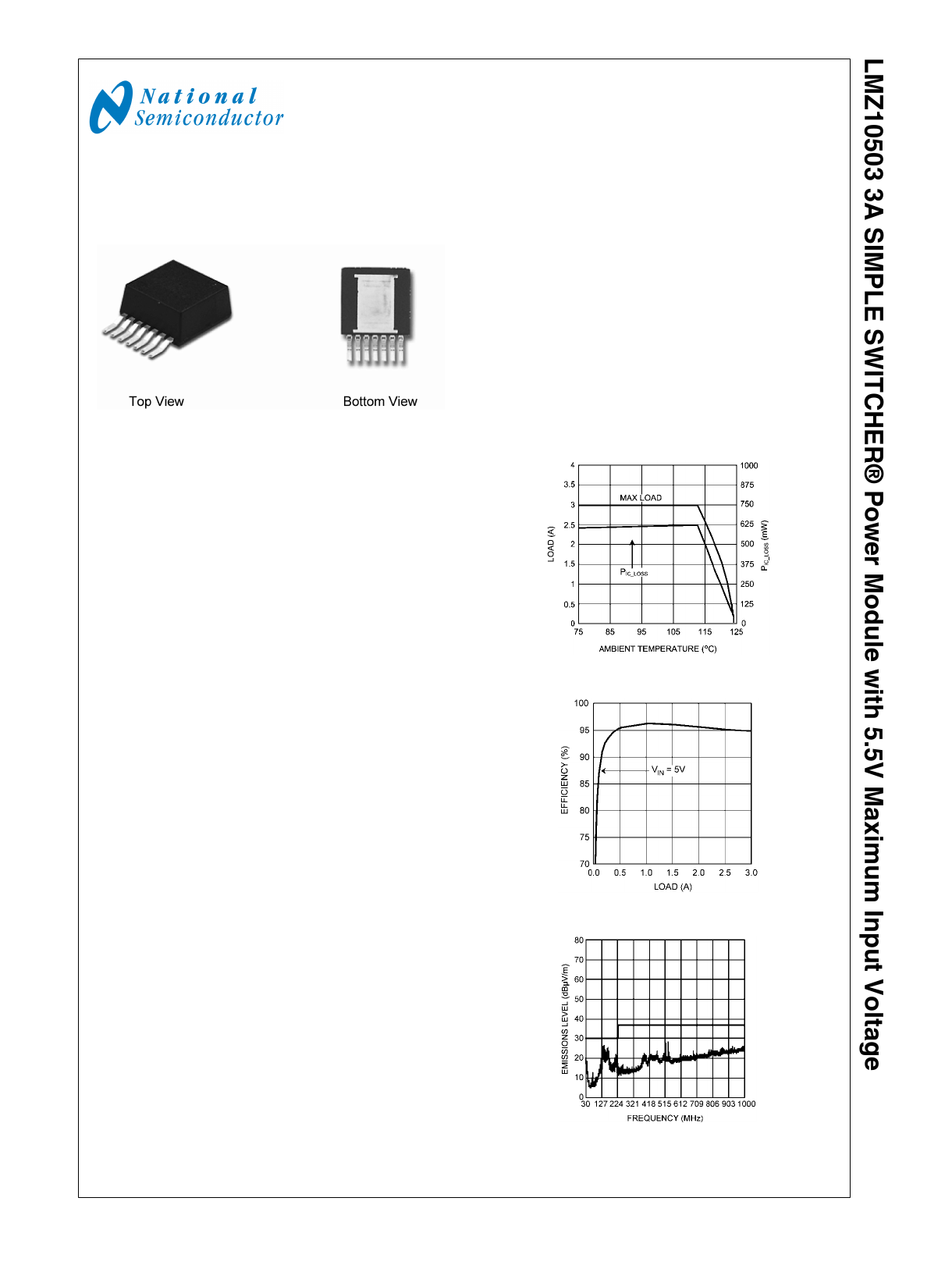
System Performance
Current Derating (VOUT = 3.3V)
Electrical Specifications
■ 15W maximum total output power
■ Up to 3A output current
■ Input voltage range 2.95V to 5.5V
■ Output voltage range 0.8V to 5V
■ ±1.63% feedback voltage accuracy over temperature
■ Efficiency up to 96%
Key Features
■ Integrated shielded inductor
■ Flexible startup sequencing using external soft-start,
tracking, and precision enable
■ Protection against in-rush currents and faults such as input
UVLO and output short-circuit
■ -40°C to +125°C junction temperature operating range
■ Single exposed pad and standard pinout for easy
mounting and manufacturing
■ Pin-to-pin compatible with
LMZ10504 (4A/20W max)
LMZ10505 (5A/25W max)
■ Fully enabled for WEBENCH® and Power Designer
Applications
■ Point-of-load conversions from 3.3V and 5V rails
■ Space constrained applications
■ Extreme temperatures/no air flow environments
■ Noise sensitive applications (i.e. transceiver, medical)
301118a5
Efficiency (VOUT = 3.3V)
30111871
Radiated Emissions (EN 55022, Class B)
301118a6
Note 1: Note 1: θ JA measured on a 2.25” x 2.25” (5.8 cm x 5.8 cm) four layer board. Refer to PCB Layout Diagrams or Evaluation Board Application Note:
AN-2022.
Note 2: Note 2: EN 55022:2006, +A1:2007, FCC Part 15 Subpart B: 2007. See Figure 5 and layout for information on device under test.
© 2010 National Semiconductor Corporation 301118
www.national.com
1 page 
www.DataSheet4U.net
Electrical Characteristics Specifications with standard typeface are for TJ = 25°C only; limits in bold face type
apply over the operating junction temperature range TJ of -40°C to 125°C. Minimum and maximum limits are guaranteed through
test, design, or statistical correlation. Typical values represent the most likely parametric norm at TJ = 25°C, and are provided for
reference purposes only. VIN = VEN = 3.3V, unless otherwise indicated in the conditions column.
Symbol
Parameter
Conditions
Min
(Note 7)
Typ Max
(Note 8) (Note 7) Units
PERFORMANCE PARAMETERS
ΔVOUT
Output Voltage Ripple
Refer to Table 3
VOUT = 2.5V
Bandwidth Limit = 2 MHz
7 mVpk-pk
ΔVOUT
Output Voltage Ripple
Refer to Table 5
Bandwidth Limit = 20 MHz
5 mVpk-pk
ΔVFB / VFB
Feedback Voltage Line Regulation
ΔVOUT / VOUT Output Voltage Line Regulation
ΔVFB / VFB
ΔVOUT / VOUT
Feedback Voltage Load Regulation
Output Voltage Load Regulation
Efficiency
ΔVIN = 2.95V to 5.5V
IOUT = 0A
ΔVIN = 2.95V to 5.5V
IOUT = 0A, VOUT = 2.5V
IOUT = 0A to 3A
IOUT = 0A to 3A
VOUT = 2.5V
0.04 %
0.04 %
0.25 %
0.25 %
VOUT = 3.3V
VOUT = 2.5V
η Peak Efficiency (1A) VIN = 5V
VOUT = 1.8V
VOUT = 1.5V
VOUT = 1.2V
VOUT = 0.8V
VOUT = 2.5V
VOUT = 1.8V
η
Peak Efficiency (1A) VIN = 3.3V
VOUT = 1.5V
VOUT = 1.2V
VOUT = 0.8V
VOUT = 3.3V
VOUT = 2.5V
η
Full Load Efficiency (3A) VIN = 5V
VOUT = 1.8V
VOUT = 1.5V
VOUT = 1.2V
VOUT = 0.8V
VOUT = 2.5V
VOUT = 1.8V
η
Full Load Efficiency (3A) VIN = 3.3V
VOUT = 1.5V
VOUT = 1.2V
VOUT = 0.8V
96.3
94.9
93.3
92.2
90.5
86.9
95.7
94.0
92.9
91.3
87.9
94.8
93
90.8
89.3
87.1
82.3
92.4
89.8
88.2
85.9
80.8
%
%
%
%
Note 3: θ JA measured on a 2.25” x 2.25” (5.8 cm x 5.8 cm) four layer board, with one ounce copper, thirty six 10mil thermal vias, no air flow, and 1W power
dissipation. Refer to PCB Layout Diagrams or Evaluation Board Application Note: AN-2022.
Note 4: EN 55022:2006, +A1:2007, FCC Part 15 Subpart B: 2007. See Table 9 and layout for information on device under test.
Note 5: Absolute Maximum Ratings are limits beyond which damage to the device may occur. Operating Ratings are conditions under which operation of the
device is intended to be functional. For guaranteed specifications and test conditions, see the Electrical Characteristics.
Note 6: The human body model is a 100 pF capacitor discharged through a 1.5 kΩ resistor into each pin. Test method is per JESD22-AI14S.
Note 7: Min and Max limits are 100% production tested at an ambient temperature (TA) of 25°C. Limits over the operating temperature range are guaranteed
through correlation using Statistical Quality Control (SQC) methods. Limits are used to calculate National’s Average Outgoing Quality Level (AOQL).
Note 8: Typical numbers are at 25°C and represent the most likely parametric norm.
5 www.national.com
5 Page 
www.DataSheet4U.net
TABLE 1. Recommended Output Filter Capacitors
CO (µF)
22
47
47
47
100
100
100
150
330
470
Voltage (V), RESR (mΩ)
6.3, < 5
6.3, < 5
6.3, < 5
10.0, < 5
6.3, < 5
6.3, 50
6.3, 25
6.3, 18
6.3, 18
6.3, 23
Make
Ceramic, X5R
Ceramic, X5R
Ceramic, X5R
Ceramic, X5R
Ceramic, X5R
Tantalum
Organic Polymer
Organic Polymer
Organic Polymer
Niobium Oxide
Manufacturer
TDK
TDK
TDK
TDK
TDK
AVX
Sanyo
Sanyo
Sanyo
AVX
Part Number
Case Size
C3216X5R0J226M
1206
C3216X5R0J476M
1206
C3225X5R0J476M
1210
C3225X5R1A476M
1210
C3225X5R0J107M
1210
TPSD157M006#0050 D, 7.5 x 4.3 x 2.9 mm
6TPE100MPB2 B2, 3.5 x 2.8 x 1.9 mm
6TPE150MIC2
C2, 6.0 x 3.2 x 1.8 mm
6TPE330MIL
D3L, 7.3 x 4.3 x 2.8 mm
NOME37M006#0023 E, 7.3 x 4.3 x 4.1 mm
Output Voltage Setting
A resistor divider network from VOUT to the FB pin determines
the desired output voltage as follows:
operation is 30° to 60° of phase margin, with a bandwidth of
100 kHz ±20 kHz.
Rfbt is defined based on the voltage loop requirements and
Rfbb is then selected for the desired output voltage. Resistors
are normally selected as 0.5% or 1% tolerance. Higher accu-
racy resistors such as 0.1% are also available.
The feedback voltage (at VOUT = 2.5V) is accurate to within
-2.5% / +2.5% over temperature and over line and load reg-
ulation. Additionally, the LMZ10503 contains error nulling
circuitry to substantially eliminate the feedback voltage vari-
ation over temperature as well as the long term aging effects
of the internal amplifiers. In addition the zero nulling circuit
dramatically reduces the 1/f noise of the bandgap amplifier
and reference. The manifestation of this circuit action is that
the duty cycle will have two slightly different but distinct op-
erating points, each evident every other switching cycle.
Loop Compensation
The LMZ10503 preserves flexibility by integrating the control
components around the internal error amplifier while utilizing
three small external compensation components from VOUT to
FB. An integrated type II (two pole, one zero) voltage-mode
compensation network is featured. To ensure stability, an ex-
ternal resistor and small value capacitor can be added across
the upper feedback resistor as a pole-zero pair to complete a
type III (three pole, two zero) compensation network. The
compensation components recommended in Table 2 provide
type III compensation at an optimal control loop performance.
The typical phase margin is 45° with a bandwidth of 80 kHz.
Calculated output capacitance values not listed in Table 2
should be verified before designing into production. A detailed
application note is available to provide verification support,
AN-2013. In general, calculated output capacitance values
below the suggested value will have reduced phase margin
and higher control loop bandwidth. Output capacitance val-
ues above the suggested values will experience a lower
bandwidth and increased phase margin. Higher bandwidth is
associated with faster system response to sudden changes
such as load transients. Phase margin changes the charac-
teristics of the response. Lower phase margin is associated
with underdamped ringing and higher phase margin is asso-
ciated with overdamped response. Losing all phase margin
will cause the system to be unstable; an optimized area of
30111848
TABLE 2. LMZ10503 Compensation Component Values
VIN CO (µF) ESR (mΩ)
Rfbt Ccomp Rcomp
(V) Min Max (kΩ) (pF) (kΩ)
22 2 20 143 39 8.06
47 2 20 100 100 8.25
100 1 10 71.5 180 4.32
150
5.0
150
1 5 56.2 270 2.1
10 25 59 270 10.8
150 26 50 66.5 270 23.7
220 15 30 53.6 360 14
220 31 60 59 360 30.1
22 2 20 100 56.2 5.62
47 2 20 66.5 150 5.49
100 1 10 45.3 270 2.8
150
3.3
150
1 5 40.2 360 1.5
10 25 40.2 360 7.32
150 26 50 43.2 360 15.4
220 15 30 40.2 470 10.5
220 31 60 40.2 470 20.5
Note: In the special case where the output voltage is 0.8V, it is recom-
mended to remove Rfbb and keep Rfbt, Rcomp, and Ccomp for a type III
compensation.
11 www.national.com
11 Page | ||
| Páginas | Total 22 Páginas | |
| PDF Descargar | [ Datasheet LMZ10503.PDF ] | |
Hoja de datos destacado
| Número de pieza | Descripción | Fabricantes |
| LMZ10500 | LMZ10500 650-mA SIMPLE SWITCHER Nano Module With 5.5-V Maximum Input Voltage (Rev. F) | Texas Instruments |
| LMZ10500 | 650mA SIMPLE SWITCHER Nano Module | National Semiconductor |
| LMZ10501 | LMZ10501 1-A SIMPLE SWITCHER Nano Module With 5.5-V Maximum Input Voltage (Rev. F) | Texas Instruments |
| LMZ10501 | 1A SIMPLE SWITCHER Nano Module | National Semiconductor |
| Número de pieza | Descripción | Fabricantes |
| SLA6805M | High Voltage 3 phase Motor Driver IC. |
Sanken |
| SDC1742 | 12- and 14-Bit Hybrid Synchro / Resolver-to-Digital Converters. |
Analog Devices |
|
DataSheet.es es una pagina web que funciona como un repositorio de manuales o hoja de datos de muchos de los productos más populares, |
| DataSheet.es | 2020 | Privacy Policy | Contacto | Buscar |