|
|
PDF K9K8G08U1D Data sheet ( Hoja de datos )
| Número de pieza | K9K8G08U1D | |
| Descripción | 4Gb D-die NAND Flash | |
| Fabricantes | Samsung | |
| Logotipo |  |
|
Hay una vista previa y un enlace de descarga de K9K8G08U1D (archivo pdf) en la parte inferior de esta página. Total 30 Páginas | ||
|
No Preview Available !
www.DataSheet4U.net
Rev.0.2, May. 2010
K9F4G08U0D
K9K8G08U0D
K9K8G08U1D
K9WAG08U1D
Advance
4Gb D-die NAND Flash
Single-Level-Cell (1bit/cell)
datasheet
SAMSUNG ELECTRONICS RESERVES THE RIGHT TO CHANGE PRODUCTS, INFORMATION AND
SPECIFICATIONS WITHOUT NOTICE.
Products and specifications discussed herein are for reference purposes only. All information discussed
herein is provided on an "AS IS" basis, without warranties of any kind.
This document and all information discussed herein remain the sole and exclusive property of Samsung
Electronics. No license of any patent, copyright, mask work, trademark or any other intellectual property
right is granted by one party to the other party under this document, by implication, estoppel or other-
wise.
Samsung products are not intended for use in life support, critical care, medical, safety equipment, or
similar applications where product failure could result in loss of life or personal or physical harm, or any
military or defense application, or any governmental procurement to which special terms or provisions
may apply.
For updates or additional information about Samsung products, contact your nearest Samsung office.
All brand names, trademarks and registered trademarks belong to their respective owners.
ⓒ 2010 Samsung Electronics Co., Ltd. All rights reserved.
-1-
1 page 
www.DataSheet4U.net
K9F4G08U0D K9K8G08U1D
K9K8G08U0D K9WAG08U1D
datasheet
1.4 Pin Configuration (TSOP1)
N.C
N.C
N.C
N.C
N.C
N.C
R/B1
RE
CE1
N.C
N.C
Vcc
Vss
N.C
N.C
CLE
ALE
WE
WP
N.C
N.C
N.C
N.C
N.C
1
2
3
4
5
6
7
8
9
10
11
12
13
14
15
16
17
18
19
20
21
22
23
24
K9F4G08U0D-SCB0/SIB0
K9K8G08U0D-SCB0/SIB0
48-pin TSOP1
Standard Type
12mm x 20mm
48 N.C
47 N.C
46 N.C
45 N.C
44 I/O7
43 I/O6
42 I/O5
41 I/O4
40 N.C
39 N.C
38 N.C
37 Vcc
36 Vss
35 N.C
34 N.C
33 N.C
32 I/O3
31 I/O2
30 I/O1
29 I/O0
28 N.C
27 N.C
26 N.C
25 N.C
Advance Rev. 0.2
FLASH MEMORY
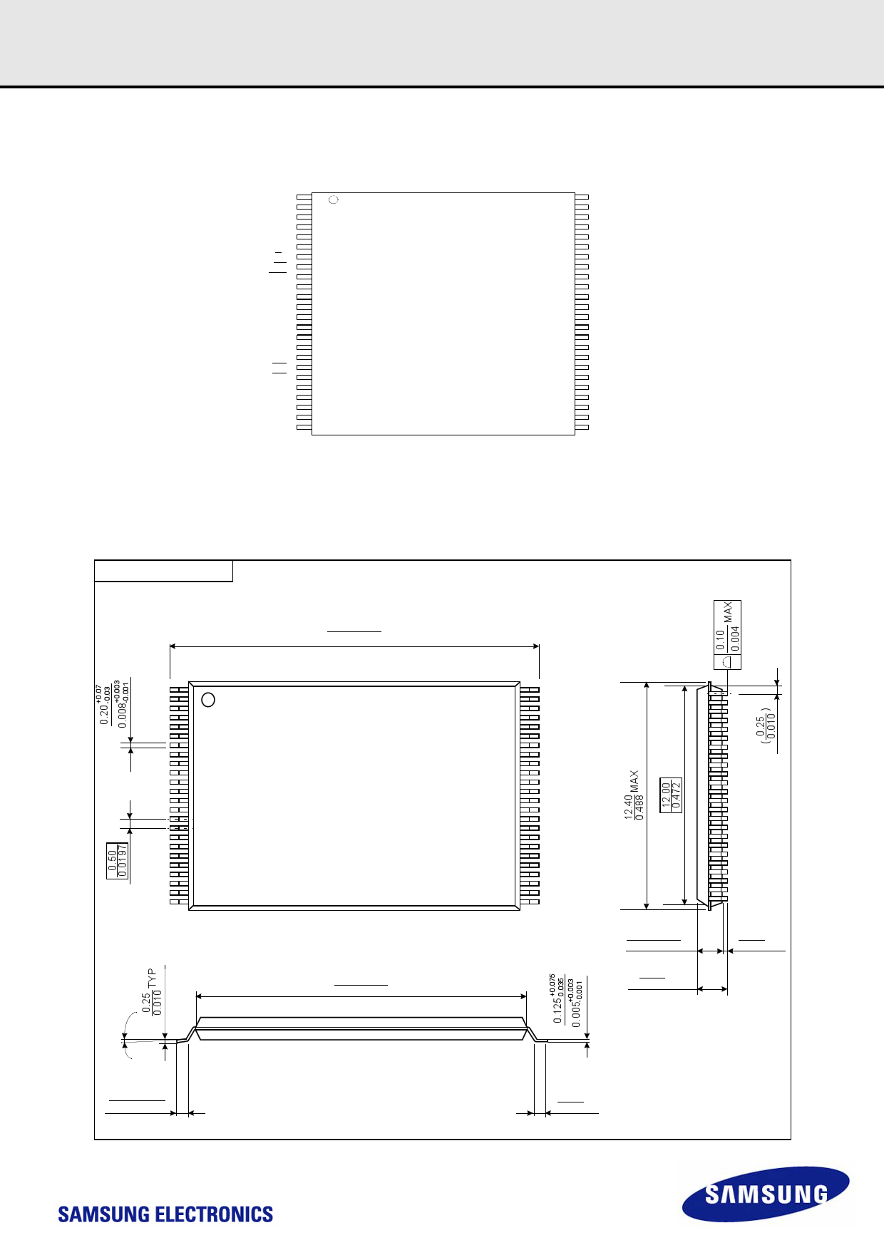
1.4.1 PACKAGE DIMENSIONS
48-PIN LEAD FREE PLASTIC THIN SMALL OUT-LINE PACKAGE TYPE(I)
48 - TSOP1 - 1220F
20.00±0.20
0.787±0.008
#1 #48
Unit :mm/Inch
#24
0~8°
0.45~0.75
0.018~0.030
18.40±0.10
0.724±0.004
#25
1.00±0.05
0.039±0.002
01..02407MAX
0.05
0.002
MIN
(
0.50
0.020
)
-5-
5 Page 
www.DataSheet4U.net
K9F4G08U0D K9K8G08U1D
K9K8G08U0D K9WAG08U1D
datasheet
Advance Rev. 0.2
FLASH MEMORY
2.4 Valid Block
Parameter
K9F4G08U0D
K9K8G08U0D
K9K8G08U1D
K9WAG08U1D
Symbol
NVB
Min
4,016
8,032
16,064
Typ.
-
Max
4,096
8,192
16,384
Unit
Blocks
NOTE :
1) The device may include initial invalid blocks when first shipped. Additional invalid blocks may develop while being used. The number of valid blocks is presented with both
cases of invalid blocks considered. Invalid blocks are defined as blocks that contain one or more bad bits. Do not erase or program factory-marked bad blocks. Refer to the
attached technical notes for appropriate management of invalid blocks.
2) The 1st block, which is placed on 00h block address, is guaranteed to be a valid block up to 1K program/erase cycles with 1bit/528Byte ECC.
3) The number of valid block is on the basis of single plane operations, and this may be decreased with two plane operations.
2.5 Ac Test Condition
(K9XXG08UXD-XCB0 :TA=0 to 70°C, K9F4G08UXD-XIB0:TA=-40 to 85°C, K9XXG08UXD: Vcc=2.7V~3.6V unless otherwise noted)
Parameter
K9XXG08UXD
Input Pulse Levels
0V to Vcc
Input Rise and Fall Times
5ns
Input and Output Timing Levels
Vcc/2
Output Load
1 TTL GATE and CL=50pF
2.6 Capacitance(TA=25°C, VCC=3.3V, f=1.0MHz)
Item
Input/Output Capacitance
Input Capacitance
Symbol
CI/O
CI/O(W)*
CIN
CIN(W)*
Test Condition
VIL=0V
VIL=0V
VIN=0V
VIN=0V
Min
-
-
-
-
Max
8
5
8
5
Unit
pF
pF
pF
pF
NOTE :
1) Capacitance is periodically sampled and not 100% tested.
2) CI/O(W)* and CIN(W)* are tested at wafer level.
2.7 Mode Selection
CLE
ALE
CE
WE
HL L
LHL
HL L
LHL
LLL
L L LH
XXXX
XXXX
XXXX
X X(1) X
X
XXHX
NOTE :
1) X can be VIL or VIH.
2) WP should be biased to CMOS high or CMOS low for standby.
RE WP
Mode
HX
Command Input
Read Mode
HX
Address Input(5clock)
HH
Command Input
Write Mode
HH
Address Input(5clock)
H H Data Input
X Data Output
H X During Read(Busy)
X H During Program(Busy)
X H During Erase(Busy)
X L Write Protect
X
0V/VCC(2)
Stand-by
- 11 -
11 Page | ||
| Páginas | Total 30 Páginas | |
| PDF Descargar | [ Datasheet K9K8G08U1D.PDF ] | |
Hoja de datos destacado
| Número de pieza | Descripción | Fabricantes |
| K9K8G08U1B | FLASH MEMORY | Samsung |
| K9K8G08U1D | 4Gb D-die NAND Flash | Samsung |
| K9K8G08U1E | 4Gb E-die NAND Flash | Samsung |
| K9K8G08U1M | 512M x 8 Bits / 1G x 8 Bits NAND Flash Memory | Samsung |
| Número de pieza | Descripción | Fabricantes |
| SLA6805M | High Voltage 3 phase Motor Driver IC. |
Sanken |
| SDC1742 | 12- and 14-Bit Hybrid Synchro / Resolver-to-Digital Converters. |
Analog Devices |
|
DataSheet.es es una pagina web que funciona como un repositorio de manuales o hoja de datos de muchos de los productos más populares, |
| DataSheet.es | 2020 | Privacy Policy | Contacto | Buscar |
