|
|
|
PDF PSC5A12-7iR Data sheet ( Hoja de datos )
| Número de pieza | PSC5A12-7iR | |
| Descripción | Positive Switching Regulators | |
| Fabricantes | Power-One AG | |
| Logotipo | ||
Hay una vista previa y un enlace de descarga de PSC5A12-7iR (archivo pdf) en la parte inferior de esta página. Total 13 Páginas | ||
|
No Preview Available !
www.DataSheet.co.kr
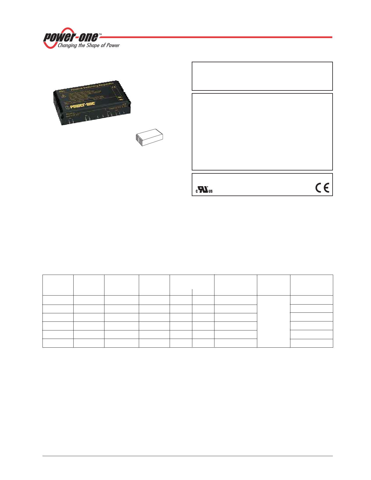
PSC Series Extended Data Sheet
Positive Switching Regulators (Industrial)
32
1.3"
88 151
3.5" 5.9"
Input voltage up to 80 VDC
Single output of 5.1 - 36 VDC
No input to output isolation
• High efficiency up to 96%
• Wide input voltage range
• Low input to output differential voltage
• Very good dynamic properties
• Input undervoltage lock-out
• External output voltage adjustment and inhibit
• Two temperature ranges
• Continuous no-load and short-circuit proof
• No derating
Safety according to IEC/EN 60950
Summary
The PSC series of positive switching regulators is designed
as power supply modules for electronic systems. Their ma-
jor advantages include a high level of efficiency that re-
mains virtually constant over the entire input voltage range,
high reliability, low ripple and excellent dynamic response.
Modules with input voltages up to 80 V are specially de-
signed for secondary switched and battery driven applica-
tions. The case design allows operation at nominal load up
to 71°C without additional cooling.
Model Selection and Key Data
Table 1: Type survey
Output
voltage
Vo nom [V]
5.1
Output
current
Io nom [A]
12
Input
voltage range
Vi [V] 1
7 - 40
Input
voltage
Vi nom [V]
20
Efficiency 2
hmin [%] htyp [%]
82 83
Type
designation
PSC 5A12-7iR
Options
-9, L, P, C, D
5.1
10
8 - 80
40 76 79 PSC 5A10-7iR
12 8 15 - 80 40 88 89 PSC 128-7iR
15 8 19 - 80 40 90 91 PSC 158-7iR
24 8 29 - 80 50 93 94 PSC 248-7iR
36 8 42 - 80 60 95 96 PSC 368-7iR
1 See: Electrical Input Data: DVio min (min. differential voltage Vi – Vo).
2 Efficiency at Vi nom and Io nom.
Non standard input/output configurations or special custom adaptions are available on request.
Superseded
old type
(phased-out)
PSR 512-7
PSR 510-7
PSR 128-7
PSR 158-7
PSR 248-7
PSR 368-7
Table of Contents
Page
Summary .......................................................................... 1
Model Selection and Key Data ......................................... 1
Part Number Description ................................................. 2
Functional Description ..................................................... 2
Electrical Input Data ......................................................... 3
Electrical Output Data ...................................................... 4
Auxiliary Functions ........................................................... 6
Page
Electromagnetic Compatibility (EMC) .............................. 7
Immunity to Environmental Conditions ............................ 8
Mechanical Data .............................................................. 9
Safety and Installation Instructions ................................ 10
Description of Options ................................................... 11
Accessories ................................................................... 12
EC-Declaration of Conformity ........................................ 13
REV. MAY 12, 2004
Page 1 of 13
Datasheet pdf - http://www.DataSheet4U.net/
1 page 
www.DataSheet.co.kr
PSC Series Extended Data Sheet
Positive Switching Regulators (Industrial)
Vo
Vod
DVo I
05010
DVo I
Io/Io nom
1
td
Vod
td
t
0
≥10 µs
Fig. 3
Dynamic load regulation.
≥10 µs
t
Parallel and Series Connection
Outputs of equal nominal voltages can be parallel-con-
nected. However, the use of a single unit with higher output
power, because of its power dissipation, is always a better
solution.
In parallel-connected operation, one or several outputs may
operate continuously at their current limit knee-point which
will cause an increase of the heat generation. Conse-
quently, the max. ambient temperature value should be re-
duced by 10 K.
Outputs can be series-connected with any other module. In
series-connection the maximum output current is limited by
the lowest current limitation. Electrically separated source
voltages are needed for each module!
Thermal Considerations
When a switching regulator is located in free, quasi-station-
ary air (convection cooling) at a temperature TA = 71°C and
is operated at its nominal output current Io nom, the case
temperature TC will be about 95°C after the warm-up
phase, measured at the Measuring point of case tempera-
ture TC (see: Mechanical Data).
Under practical operating conditions, the ambient tempera-
ture TA may exceed 71°C, provided additional measures
(heat sink, fan, etc.) are taken to ensure that the case tem-
perature TC does not exceed its maximum value of 95°C.
Example: Sufficient forced cooling allows TA max = 85°C. A
simple check of the case temperature TC (TC ≤ 95°C) at full
load ensures correct operation of the system.
Io/Io nom
Forced cooling
1.0
0.9
0.8
0.7 Convection cooling
0.6
0.5
0.4
0.3
0.2
0.1
0
TA min 50 60 70 80 90
Fig. 4
Output current derating versus temperature
TC max
100 TA [˚C]
Short Circuit Behaviour
A constant current limitation circuit holds the output current
almost constant whenever an overload or a short circuit is
applied to the regulator's output. It acts self-protecting and
recovers – in contrary to the fold back method – automati-
cally after removal of the overload or short circuit condition.
Vo/Vo nom
1.2
05033
1.0
0.8
Io L
0.6
0.4
0.2
0
Io/Io nom
0.2 0.4 0.6 0.8 1.0 1.2 1.4
Fig. 5
Overload, short-circuit behaviour Vo versus Io.
Output Protection
A voltage suppressor diode which in worst case conditions
fails into a short circuit (or a thyristor crowbar, option C)
protects the output against an internally generated over-
voltage. Such an overvoltage could occur due to a failure of
either the control circuit or the switching transistor. The out-
put protection is not designed to withstand externally ap-
plied overvoltages. The user should ensure that systems
with Power-One power supplies, in the event of a failure, do
not result in an unsafe condition (fail-safe).
REV. MAY 12, 2004
Page 5 of 13
Datasheet pdf - http://www.DataSheet4U.net/
5 Page 
www.DataSheet.co.kr
PSC Series Extended Data Sheet
Positive Switching Regulators (Industrial)
Description of Options
-9 Extended Temperature Range
The operational ambient temperature range is extended to
TA = –40 to 71°C. (TC = –40 to 95°C, TS = –55 to 100°C.)
P Potentiometer
Option P excludes R function. The output voltage Vo can be
adjusted with a screwdriver in the range from 0.92 - 1.08 of
the nominal output voltage Vo nom.
However, the minimum differential voltage DVi o min between
input and output voltages as specified in: Electrical Input
Data should be maintained.
L Input Filter
Option L is recommended to reduce superimposed inter-
ference voltages and to prevent oscillations, if input lines
exceed approx. 5 m in total length. The fundamental wave
(approx. 120 kHz) of the reduced interference voltage be-
tween Vi+ and Gi– has, with an input line inductance of
5 µH, a maximum magnitude of 4 mVAC. A reduction can
be achieved by insertion of a capacitor across the input
(e.g. plastic foil between Vi+ and Gi–).
The input impedance of the switching regulator at 120 kHz
is about 3.5 Ω. The harmonics are small in comparison with
the fundamental wave. See also: Electrical Input Data: RFI.
With option L, the maximum permissible additionally su-
perimposed ripple ui of the input voltage (rectifier mode) at
a specified input frequency f i has the following values:
Units with max input voltage 40 V:
ui max = 12 Vpp at 100 Hz or Vpp = 1200 Hz/f i • 1V
Units with max input voltage 80 V:
ui max = 22 Vpp at 100 Hz or Vpp = 2200 Hz/f i • 1V
C Crowbar
This option is recommended to protect the load against
power supply malfunction, but it is not designed to sink ex-
ternal currents.
A fixed-value monitoring circuit checks the output voltage
Vo. When the trigger voltage Vo c is reached, the thyristor
crowbar triggers and disables the output. It may be deacti-
vated by removal of the input voltage. In case of a switching
transistor defect, an internal fuse prevents excessive cur-
rent.
Note: As a central overvoltage protection device, the crow-
bar is usually connected to the external load via distributed
inductance of the lines. For this reason, the overvoltage at
the load can temporarily exceed the trigger voltage Vo c. De-
pending on the application, further decentralized over-
voltage protection elements may have to be used addition-
ally.
Table 10: Crowbar trigger levels
Characteristics
Conditions
Vo c Trigger voltage Vi min - Vi max
Io = 0 - Io nom
t s Delay time
TC min - TC max
5.1 V
min max
5.8 6.8
1.5
12 V
min max
13.5 16
1.5
15 V
min max
16.5 19
1.5
24 V
min max
27 31
1.5
36 V
min max
40 45.5
1.5
Unit
V
µs
D Save Data Input Undervoltage Monitor
Note: Output instead of input undervoltage monitor is
available on request (Option D1).
Terminal D and Go– are connected to a normally conduct-
ing field effect transistor (JFET). The switching characteris-
tics of the option D output are shown in fig. Definition of Vt
and VH. A 0.5 W Zener diode provides protection against
overvoltages.
The voltage Vt can be externally adjusted with a trim poten-
tiometer by means of a screwdriver. The hysteresis VH of Vt
is <2%. Terminal D stays low for a minimum time tlow min, in
order to prevent any oscillation. Vt can be set to a value
between Vi min and Vi max. Please note that the JFET be-
comes conductive when VD increases above 7 V approx.
Vi +
Vt JFET
D ID
8.2 V VD
10 kΩ
11025
100 pF
+5 V
Gi – Go –
Fig. 13
Test circuit with definition of voltage VD and current ID
REV. MAY 12, 2004
Page 11 of 13
Datasheet pdf - http://www.DataSheet4U.net/
11 Page | ||
| Páginas | Total 13 Páginas | |
| PDF Descargar | [ Datasheet PSC5A12-7iR.PDF ] | |
Hoja de datos destacado
| Número de pieza | Descripción | Fabricantes |
| PSC5A12-7iR | 6...12 A Switching Regulators | Power-One |
| PSC5A12-7iR | Positive Switching Regulators | Power-One AG |
| PSC5A12-7iR | Positive Switching Regulators | Melcher AG |
| Número de pieza | Descripción | Fabricantes |
| SLA6805M | High Voltage 3 phase Motor Driver IC. |
Sanken |
| SDC1742 | 12- and 14-Bit Hybrid Synchro / Resolver-to-Digital Converters. |
Analog Devices |
|
DataSheet.es es una pagina web que funciona como un repositorio de manuales o hoja de datos de muchos de los productos más populares, |
| DataSheet.es | 2020 | Privacy Policy | Contacto | Buscar |