|
|
|
PDF MRFE6VP61K25HSR6 Data sheet ( Hoja de datos )
| Número de pieza | MRFE6VP61K25HSR6 | |
| Descripción | RF Power Field Effect Transistors | |
| Fabricantes | Freescale Semiconductor | |
| Logotipo | ||
Hay una vista previa y un enlace de descarga de MRFE6VP61K25HSR6 (archivo pdf) en la parte inferior de esta página. Total 13 Páginas | ||
|
No Preview Available !
www.DataSheet.co.kr
Freescale Semiconductor
Technical Data
RF Power Field Effect Transistors
High Ruggedness N--Channel
Enhancement--Mode Lateral MOSFETs
These high ruggedness devices are designed for use in high VSWR industrial
(including laser and plasma exciters), broadcast (analog and digital), aerospace
and radio/land mobile applications. They are unmatched input and output
designs allowing wide frequency range utilization, between 1.8 and 600 MHz.
• Typical Performance: VDD = 50 Volts, IDQ = 100 mA
Signal Type
Pout
(W)
f Gps ηD IRL
(MHz) (dB) (%) (dB)
Pulsed (100 μsec, 1250 Peak
20% Duty Cycle)
230
24.0 74.0
--14
CW
1250 CW
230
22.9 74.6
--15
Document Number: MRFE6VP61K25H
Rev. 1, 1/2011
MRFE6VP61K25HR6
MRFE6VP61K25HSR6
1.8--600 MHz, 1250 W CW, 50 V
LATERAL N--CHANNEL
BROADBAND
RF POWER MOSFETs
• Capable of Handling a Load Mismatch of 65:1 VSWR, @ 50 Vdc,
230 MHz, at all Phase Angles, Designed for Enhanced Ruggedness,
1250 Watts Pulsed Peak Power, 20% Duty Cycle, 100 μsec
• Capable of 1250 Watts CW Operation
Features
• Unmatched Input and Output Allowing Wide Frequency Range Utilization
• Device can be used Single--Ended or in a Push--Pull Configuration
• Qualified Up to a Maximum of 50 VDD Operation
• Characterized from 30 V to 50 V for Extended Power Range
• Suitable for Linear Application with Appropriate Biasing
• Integrated ESD Protection with Greater Negative Gate--Source Voltage
Range for Improved Class C Operation
• Characterized with Series Equivalent Large--Signal Impedance Parameters
• RoHS Compliant
• In Tape and Reel. R6 Suffix = 150 Units, 56 mm Tape Width, 13 inch Reel.
For R5 Tape and Reel options, see p. 12.
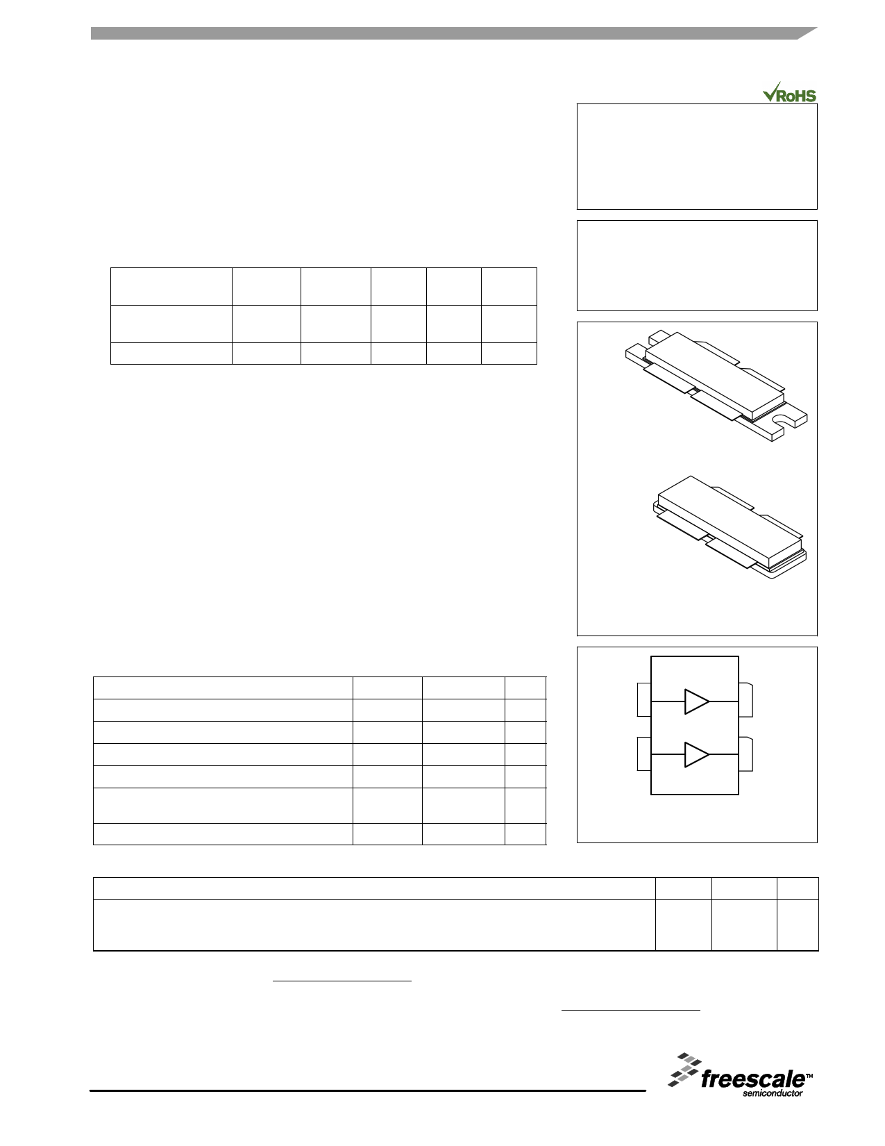
CASE 375D--05, STYLE 1
NI--1230
MRFE6VP61K25HR6
CASE 375E--04, STYLE 1
NI--1230S
MRFE6VP61K25HSR6
PARTS ARE PUSH--PULL
Table 1. Maximum Ratings
Rating
Drain--Source Voltage
Gate--Source Voltage
Storage Temperature Range
Case Operating Temperature
Total Device Dissipation @ TC = 25°C
Derate above 25°C
Operating Junction Temperature (1,2)
Symbol
VDSS
VGS
Tstg
TC
PD
TJ
Value
--0.5, +125
--6.0, +10
-- 65 to +150
150
1333
6.67
225
Unit
Vdc
Vdc
°C
°C
W
W/°C
°C
RFin/VGS 3
1 RFout/VDS
RFin/VGS 4
2 RFout/VDS
(Top View)
Figure 1. Pin Connections
Table 2. Thermal Characteristics
Characteristic
Symbol Value (2,3) Unit
Thermal Resistance, Junction to Case
Case Temperature 66°C, 1250 W Pulsed, 100 μsec Pulse Width, 20% Duty Cycle, 100 mA, 230 MHz
Case Temperature 63°C, 1250 W CW, 100 mA, 230 MHz
ZθJC
RθJC
°C/W
0.03
0.15
1. Continuous use at maximum temperature will affect MTTF.
2. MTTF calculator available at http://www.freescale.com/rf. Select Software & Tools/Development Tools/Calculators to access MTTF
calculators by product.
3. Refer to AN1955, Thermal Measurement Methodology of RF Power Amplifiers. Go to http://www.freescale.com/rf.
Select Documentation/Application Notes -- AN1955.
© Freescale Semiconductor, Inc., 2010--2011. All rights reserved.
RF Device Data
Freescale Semiconductor
MRFE6VP61K25HR6 MRFE6VP61K25HSR6
1
Datasheet pdf - http://www.DataSheet4U.net/
1 page 
www.DataSheet.co.kr
TYPICAL CHARACTERISTICS
2000
1000
Ciss
100 Coss
10
Measured with ±30 mV(rms)ac @ 1 MHz
1 VGS = 0 Vdc
0 10 20 30
Crss
40 50
VDS, DRAIN--SOURCE VOLTAGE (VOLTS)
Note: Each side of device measured separately.
Figure 4. Capacitance versus Drain--Source Voltage
66
P3dB = 61.9 dBm (1553 W)
65
P2dB = 61.7 dBm (1472 W)
64
Ideal
63 P1dB = 61.3 dBm
(1333 W)
62
Actual
61
60 VDD = 50 Vdc, IDQ = 100 mA, f = 230 MHz
Pulse Width = 100 μsec, 20% Duty Cycle
59
35 36 37 38 39 40 41 42
Pin, INPUT POWER (dBm) PULSED
Figure 5. Pulsed Output Power versus
Input Power
26
VDD = 50 Vdc, IDQ = 100 mA, f = 230 MHz
25 Pulse Width = 100 μsec, 20% Duty Cycle
90
80
24 70
23
Gps
22
60
50
21
20
100
ηD
40
30
1000 2000
Pout, OUTPUT POWER (WATTS) PULSED
Figure 6. Pulsed Power Gain and Drain Efficiency
versus Output Power
26
25
VPDulDse=W50idVthdc=,
1ID0Q0
= 100
μsec,
mA, f = 230 MHz
20% Duty Cycle
24
23
22
21 50 V
20
19
40 V 45 V
18 35 V
17 VDD = 30 V
16
0 200 400 600 800 1000 1200 1400 1600
Pout, OUTPUT POWER (WATTS) PULSED
Figure 7. Pulsed Power Gain versus
Output Power
90
80
VDD = 30 V
35 V
40 V 45 V 50 V
70
60
50
40
30
VDD = 50 Vdc, IDQ = 100 mA, f = 230 MHz
Pulse Width = 100 μsec, 20% Duty Cycle
20
0 200 400 600 800 1000 1200 1400 1600
Pout, OUTPUT POWER (WATTS) PULSED
Figure 8. Pulsed Drain Efficiency versus
Output Power
26
VDD = 50 Vdc, IDQ = 100 mA, f = 230 MHz
25 Pulse Width = 100 μsec, 20% Duty Cycle
--30_C 90
25_C
80
24
TC = --30_C
23 25_C
22 Gps
21
85_C
85_C 70
60
50
40
20
ηD
19
100
30
20
1000 2000
Pout, OUTPUT POWER (WATTS) PULSED
Figure 9. Pulsed Power Gain and Drain Efficiency
versus Output Power
RF Device Data
Freescale Semiconductor
MRFE6VP61K25HR6 MRFE6VP61K25HSR6
5
Datasheet pdf - http://www.DataSheet4U.net/
5 Page 
www.DataSheet.co.kr
RF Device Data
Freescale Semiconductor
MRFE6VP61K25HR6 MRFE6VP61K25HSR6
11
Datasheet pdf - http://www.DataSheet4U.net/
11 Page | ||
| Páginas | Total 13 Páginas | |
| PDF Descargar | [ Datasheet MRFE6VP61K25HSR6.PDF ] | |
Hoja de datos destacado
| Número de pieza | Descripción | Fabricantes |
| MRFE6VP61K25HSR6 | RF Power Field Effect Transistors | Freescale Semiconductor |
| Número de pieza | Descripción | Fabricantes |
| SLA6805M | High Voltage 3 phase Motor Driver IC. |
Sanken |
| SDC1742 | 12- and 14-Bit Hybrid Synchro / Resolver-to-Digital Converters. |
Analog Devices |
|
DataSheet.es es una pagina web que funciona como un repositorio de manuales o hoja de datos de muchos de los productos más populares, |
| DataSheet.es | 2020 | Privacy Policy | Contacto | Buscar |