|
|
|
PDF CH450 Data sheet ( Hoja de datos )
| Número de pieza | CH450 | |
| Descripción | LED drive and keyboard control chip | |
| Fabricantes | ETC | |
| Logotipo | ||
Hay una vista previa y un enlace de descarga de CH450 (archivo pdf) en la parte inferior de esta página. Total 9 Páginas | ||
|
No Preview Available !
www.DataSheet.co.kr
The DataSheet of CH450 (the first)
1
LED drive and keyboard control chip CH450
English DataSheet
Version:1C
http://wch.cn
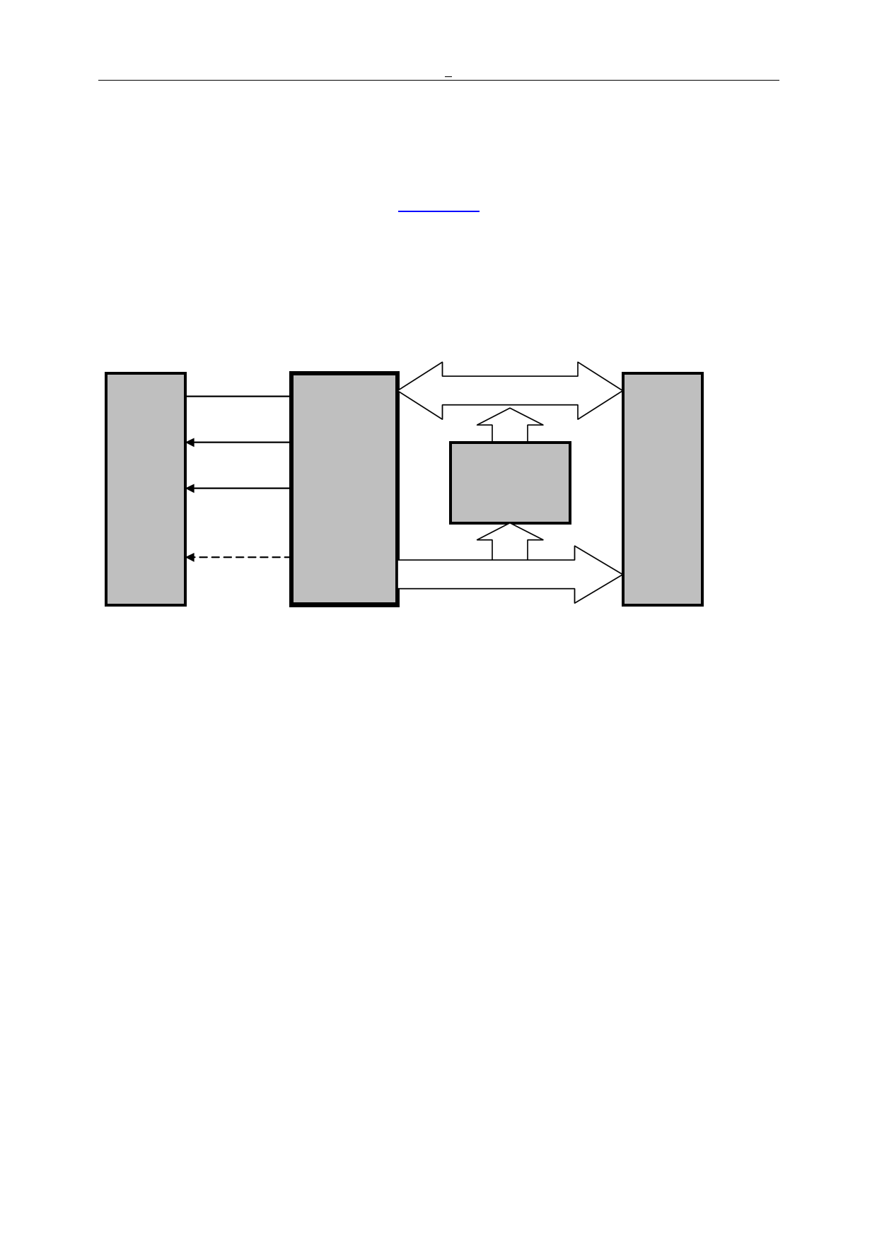
1. Introduction
CH450 is numeric LEDs display drive and keyboard scan control chip. CH450 sets clock surging
circuit internal, drives six bits numeric LEDs or forty-eight LEDs automatically. And it carries out
forty-eight keys keyboard scan. CH450 exchanges data with MCU via two wires serial interface and supplies
power-up reset signal to MCU.
SCL SEG7~SEG0
MCU
etc
SDA
INT#
RSTH
CH450 chip
(broken line
are optional)
8×6 matrix
48 keys
keyboard
DIG7~DIG2
Six bits
numeric
LEDs or
forty
eight
LEDs
2. Features
● Set display current drive layer internal, the segment current is no less than 15mA, the word current is no
less than 80mA.
● Dynamically display scan control, directly drive six bits numeric LEDs or forty eight LEDs.
● Set forty eight keys keyboard controller internal, basic on 8×6 matrix keyboard scan.
● Set pull-down resistor internal on the key pressed station, and set eliminate dithering circuit internal.
● Supplies keyboard interrupt active with low-level, supplies key-press release sign bit, to detect key is
pressed or released.
● High-speed two wires serial interface, the speed of clock varies from 0 to 4MHz,compatible with two
wires I2C bus, save pins.
● Set clock surge circuit internal, the outside supplies clock or surging equipments is no need, stand against
disturbing.
● Set clock surging circuit internal, don’t need outside to provide clock or connect surge device,
anti-jamming capability is more stronger.
● Set power-on reset internal, supplies reset output active with high-level to MCU.
● Supplies DIP20 and SOP20 package without lead, compatible with RoHS, the function and pins are
compatible with CH455 in some parts.
Datasheetpdf-htp:/www.DataSheet4U.net/
1 page 
www.DataSheet.co.kr
The DataSheet of CH450 (the first)
5
used to input data. The detail process can consult the explanation on subprogram.
The write transaction contains six processes: output start signal, output byte one, acknowledge one,
output byte two, acknowledge two and output stop signal. The start signal and stop signal is as the before,
acknowledge one and two is 1, the byte one and byte two each contains eight data bits.
The read transaction contains six processes: output start signal, output byte one, acknowledge one, input
byte two, acknowledge two, output stop signal. The start signal and stop signal is as the before, acknowledge
one and two is 1, the byte one and byte two each contains eight data bits.
In the following image, the byte one 01001000B, 48H; the byte two is 00000001B, 01H.
6. Operation command
The operation command of CH450 is divided as three groups. The start signal, stop signal, acknowledge
one and acknowledge two is same of each command. The difference of them is the byte one and the byte two
and the direction of byte two.
6.1. Set system parameter command
The output byte one of this command is 01001000B, 48H; the output byte two is
000000[KEYB][DISP]B, 00H, 01H,02H or 03H.
This command is used to set system parameter of CH450: display drive enable DISP, keyboard scan
enable KEYB. When DISP is one, allowing display output; when DISP is 0, close display drive. When
KEYB is one, allowing start keyboard scan, when KEYB is 0, close keyboard scan. The command has no
influence on the data in the inner data buffer.
6.2. Load byte data command
The byte one of this command is address 64H, 66H, 68H, 6AH, 6CH or 6EH, corresponding to six
number LEDs driven by DIG2~DIG7; the byte two is [DIG_DATA]B, the value is between 00H to 0FFH,
eight bits word data.
Load data command is used to write word data DIG_DATA to data register appointed by byte one. For
example, command data 01100100B (64H corresponding to DIG2), 01111001B shows that writes word data
79H to the first data register, and displays E driven by DIG2.
After power up reset, the data in CH450 inner data register is not sure, so before the starting, clear the
data in data register, or directly load data which will be display. The reset process has no effect on data in
data register.
6.3. Read key-press code command
The output byte of this command is 01001111B, 4FH; the low seven bits of the input byte is key-press
code.
This command is used to get the valid key-press code which is checked by CH450. It is a read
transaction, and with return data. MCU must release SDA pin (tri-state output forbid or pull-up to high-level),
then CH450 output key-press code from SDA, the valid key-press code is bit6 to bit0, the bit6 is status code,
bit5 to bit0 is scan code and key-press address.
Datasheet pdf - http://www.DataSheet4U.net/
5 Page | ||
| Páginas | Total 9 Páginas | |
| PDF Descargar | [ Datasheet CH450.PDF ] | |
Hoja de datos destacado
| Número de pieza | Descripción | Fabricantes |
| CH450 | LED drive and keyboard control chip | ETC |
| CH450FPT | SCHOTTKY BARRIER DIODE | Chenmko Enterprise |
| CH452 | Digital tube driver and keyboard control chip | ETC |
| CH455 | LED drive and keyboard control chip | ETC |
| Número de pieza | Descripción | Fabricantes |
| SLA6805M | High Voltage 3 phase Motor Driver IC. |
Sanken |
| SDC1742 | 12- and 14-Bit Hybrid Synchro / Resolver-to-Digital Converters. |
Analog Devices |
|
DataSheet.es es una pagina web que funciona como un repositorio de manuales o hoja de datos de muchos de los productos más populares, |
| DataSheet.es | 2020 | Privacy Policy | Contacto | Buscar |