|
|
|
PDF 2N6388 Data sheet ( Hoja de datos )
| Número de pieza | 2N6388 | |
| Descripción | DARLINGTON NPN SILICON POWER TRANSISTORS | |
| Fabricantes | ON Semiconductor | |
| Logotipo | ||
Hay una vista previa y un enlace de descarga de 2N6388 (archivo pdf) en la parte inferior de esta página. Total 6 Páginas | ||
|
No Preview Available !
www.DataSheet4U.com
2N6387, 2N6388
2N6388 is a Preferred Device
Plastic Medium−Power
Silicon Transistors
These devices are designed for general−purpose amplifier and
low−speed switching applications.
Features
• High DC Current Gain − hFE = 2500 (Typ) @ IC = 4.0 Adc
• Collector−Emitter Sustaining Voltage − @ 100 mAdc
VCEO(sus) = 60 Vdc (Min) − 2N6387
= 80 Vdc (Min) − 2N6388
• Low Collector−Emitter Saturation Voltage −
VCE(sat) = 2.0 Vdc (Max) @ IC
= 5.0 Adc − 2N6387, 2N6388
• Monolithic Construction with Built−In Base−Emitter Shunt Resistors
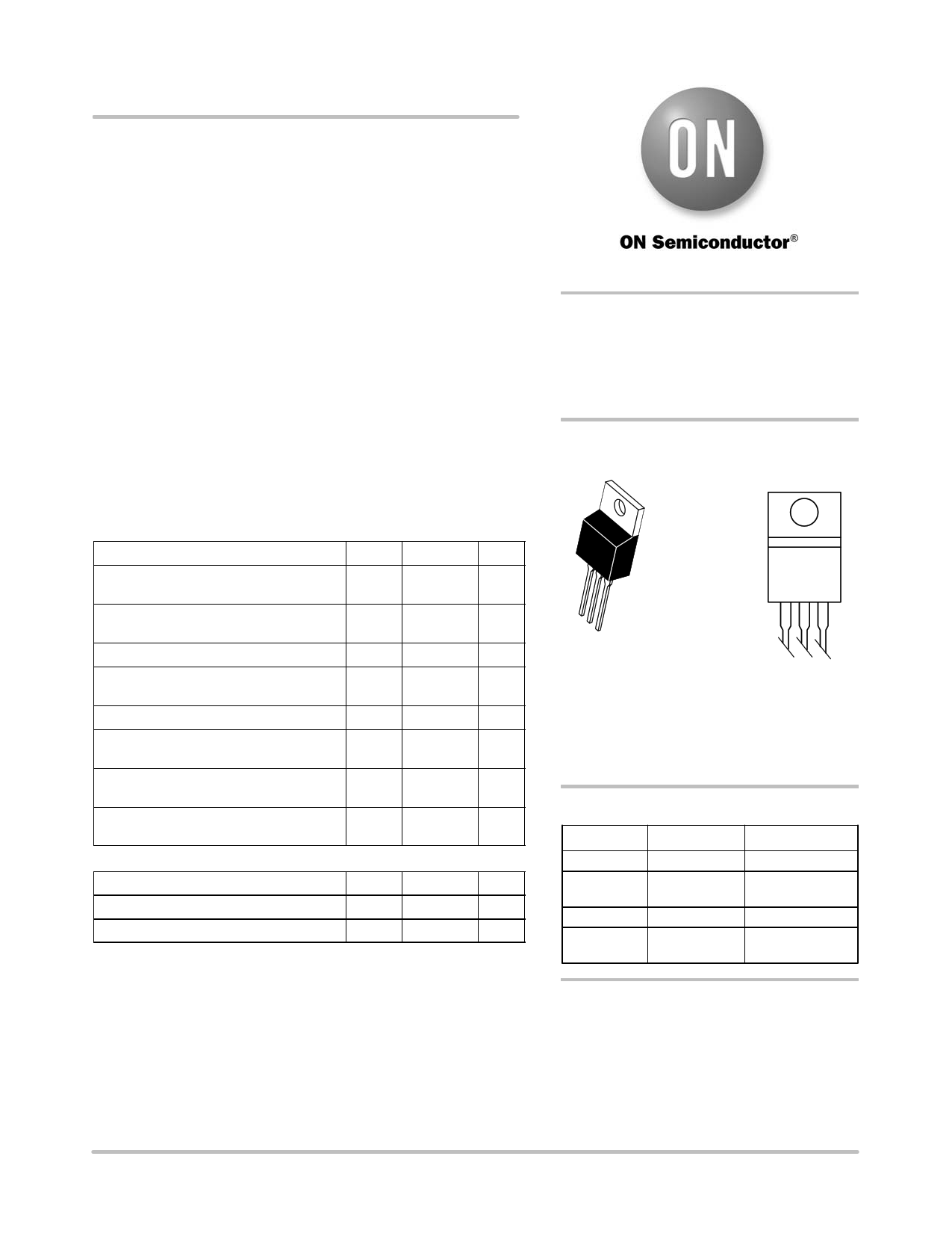
• TO−220AB Compact Package
• Pb−Free Packages are Available*
http://onsemi.com
DARLINGTON NPN SILICON
POWER TRANSISTORS
8 AND 10 AMPERES
65 WATTS, 60 − 80 VOLTS
MARKING
DIAGRAM
MAXIMUM RATINGS (Note 1)
Rating
Collector−Emitter Voltage
Symbol
2N6387 VCEO
2N6388
Value
60
80
Unit
Vdc
Collector−Base Voltage
2N6387 VCB
2N6388
60 Vdc
80
Emitter−Base Voltage
Collector Current − Continuous
− Peak
VEB 5.0 Vdc
IC 10 Adc
15
Base Current
Total Power Dissipation @ TC = 25_C
Derate above 25_C
IB 250 mAdc
PD 65 W
0.52 W/°C
Total Power Dissipation @ TA = 25_C
Derate above 25_C
Operating and Storage Junction,
Temperature Range
PD 2.0 W
0.016 W/°C
TJ, Tstg −65 to +150 °C
THERMAL CHARACTERISTICS
Characteristics
Symbol
Max
Unit
Thermal Resistance, Junction−to−Case
RqJC
1.92 _C/W
Thermal Resistance, Junction−to−Ambient RqJA
62.5 _C/W
Stresses exceeding Maximum Ratings may damage the device. Maximum
Ratings are stress ratings only. Functional operation above the Recommended
Operating Conditions is not implied. Extended exposure to stresses above the
Recommended Operating Conditions may affect device reliability.
1. Indicates JEDEC Registered Data.
1
2
3
4
TO−220AB
CASE 221A
STYLE 1
2N638xG
AYWW
2N638x = Device Code
x = 7 or 8
G = Pb−Free Package
A = Assembly Location
Y = Year
WW = Work Week
ORDERING INFORMATION
Device
Package
Shipping
2N6387
2N6387G
2N6388
2N6388G
TO−220AB
TO−220AB
(Pb−Free)
TO−220AB
TO−220AB
(Pb−Free)
50 Units / Rail
50 Units / Rail
50 Units / Rail
50 Units / Rail
Preferred devices are recommended choices for future use
and best overall value.
*For additional information on our Pb−Free strategy and soldering details, please
download the ON Semiconductor Soldering and Mounting Techniques
Reference Manual, SOLDERRM/D.
© Semiconductor Components Industries, LLC, 2006
August, 2006 − Rev. 12
1
Publication Order Number:
2N6387/D
1 page 
2N6387, 2N6388
3.0
TJ = 25°C
2.5
2.0
1.5 VBE(sat) @ IC/IB = 250
VBE @ VCE = 4.0 V
1.0
VCE(sat) @ IC/IB = 250
0.5
0.1
0.2 0.3 0.5 0.7 1.0
2.0 3.0
IC, COLLECTOR CURRENT (AMP)
Figure 10. “On” Voltages
5.0 7.0 10
+ 5.0
+ 4.0
+ 3.0
*IC/IB ≤
hFE @ VCE + 4.0 V
3
+ 2.0
25°C to 150°C
+ 1.0
0
*qVC for VCE(sat)
−55 °C to 25°C
− 1.0
− 2.0
− 3.0
− 4.0
− 5.0
0.1
qVB for VBE
0.2 0.3
25°C to 150°C
0.5 0.7 1.0
−55 °C to 25°C
2.0 3.0 5.0 7.0 10
IC, COLLECTOR CURRENT (AMP)
Figure 11. Temperature Coefficients
105
REVERSE
104
FORWARD
VCE = 30 V
103
102
TJ = 150°C
101
100 100°C
10− 1 25°C
−0.6 −0.4 −0.2
0 +0.2 +0.4 +0.6 +0.8 +1.0 +1.2 + 1.4
VBE, BASE−EMITTER VOLTAGE (VOLTS)
Figure 12. Collector Cut−Off Region
COLLECTOR
BASE
[ 8.0 k [ 120
EMITTER
Figure 13. Darlington Schematic
http://onsemi.com
5
5 Page | ||
| Páginas | Total 6 Páginas | |
| PDF Descargar | [ Datasheet 2N6388.PDF ] | |
Hoja de datos destacado
| Número de pieza | Descripción | Fabricantes |
| 2N6380 | Trans GP BJT PNP 80V 50A 3-Pin TO-63 | New Jersey Semiconductor |
| 2N6381 | Trans GP BJT PNP 100V 50A 3-Pin TO-63 | New Jersey Semiconductor |
| 2N6383 | POWER TRANSISTORS(10A/100W) | Mospec Semiconductor |
| 2N6383 | NPN DARLINGTON POWER SILICON TRANSISTOR | Microsemi Corporation |
| Número de pieza | Descripción | Fabricantes |
| SLA6805M | High Voltage 3 phase Motor Driver IC. |
Sanken |
| SDC1742 | 12- and 14-Bit Hybrid Synchro / Resolver-to-Digital Converters. |
Analog Devices |
|
DataSheet.es es una pagina web que funciona como un repositorio de manuales o hoja de datos de muchos de los productos más populares, |
| DataSheet.es | 2020 | Privacy Policy | Contacto | Buscar |