|
|
PDF TSS-IO16-E Data sheet ( Hoja de datos )
| Número de pieza | TSS-IO16-E | |
| Descripción | Van Peripheral Circuit - 16 Inputs-outputs | |
| Fabricantes | ATMEL Corporation | |
| Logotipo |  |
|
Hay una vista previa y un enlace de descarga de TSS-IO16-E (archivo pdf) en la parte inferior de esta página. Total 16 Páginas | ||
|
No Preview Available !
TSSIO16E
VAN peripheral circuit - 16 inputs-outputs
1. Features
q Management of 16 inputs-outputs (16-bit or two 8-bit configurable ports)
q VAN protocol V4.0
q 3 external wired address
q Safety mode in case of transmission loss
q Automatic adaptation to speed of bus from 8kTS/s to 250kTS/s
q CMOS 0,5µm, IO CMOS TTL compatible
q Internal power-on-reset
q Internal ring oscillator from 10 to 40MHz (for internal clock)
q 500kHz oscillator with external RC network (for safety mode clock usage)
q Supply voltage 5V±10%
q Typical power consomption 4mA
q SO28 package
2. General description / block diagram
The block diagram given below shows the organization of the circuit as two blocks: the VAN controller (block 1),
and the groups of specific functions (block 2) relative to the TSSIO16E. These are based on management of 16
inputs-outputs grouped together to form two 8-bit bi-directional programmable ports: port A and port B. The
http://www.DataSheet4U.net/
circuit thus ensures double exchange of information with the VAN bus (via the line interface) on the one hand
and the active environment on the other.
External address
Line
interface
VAN
controller
Block 1
Specific
functions
Block 2
Safety mode code
TSSIO16E
Active environment
Figure 1.
The bus data is supplied to the circuit (after shaping by the line transmitter/receiver) through 3 input lines RXD0,
RXD1 and RXD2 selected one after another when communication on one of the lines is defective (line diagnosis
system). Operation outside of the RXD0 line is referred to as in degrated mode. If perturbations persist in
reception the circuit switches to the safety mode (INT = 1) which, by default, ensures safety functions by activating
or inhibiting external circuitry. Two CONTROL and STATUS 8-bit registers, are used respectively for setting
operation to a given configuration, and for diagnosing the state of the circuit.
The write and read modes of ports A and B are determined by decoding the local address of the identifier field
in the VAN frame.
Rev. B - June. 07, 2000
1
datasheet pdf - http://www.DataSheet4U.net/
1 page 
TSSIO16E
4.3 Programming and structure of port A and B
Table below summarizes the programming of a port for the corresponding bits in the DATA, DDR and OPT bytes,
and shows the structural organization of the logic ports.
OPT_X(n)
0
0
0
0
1
DDR_X(n)
0
0
1
1
X
Table 3.
DATA_X(n)
0
1
0
1
X
programming of pin n of port X
logic input
forbidden case (even input)
logic output set to 0
logic output set to 1
forbidden case
bi-directional access
B
B PA[n]
PB[n]
http://www.DataSheet4U.net/
4.4 COMMAND and STATUS registers
These two specialized registers ensure command and monitoring functions as follows:
q Lines management according to a line diagnosis carried out constantly. This line diagnosis analyzes the
transmission state and allows a choice of the RXD0, RXD1, RXD2 inputs depending on some of the TIME-
OUT’s (STO, MTO, LTO and SLTO);
q Accesses management to common peripherals shared by several circuits.
These registers have the following structure:
Protection bit or occupation flag
Surveillance or mode bit
User module number
Selection/status input lines
Figure 4.
4.4.1 Management of RXD0, RXD1, RXD2 lines and common access to peripherals
The purpose of line diagnosis is to find a line that operates before exiting from NORMAL mode to enter SAFETY
mode. This diagnosis is covered by events or TIME-OUT’s with which the time-out’s are associated.
Rev. B - June. 07, 2000
5
datasheet pdf - http://www.DataSheet4U.net/
5 Page 
TSSIO16E
symbol
VIL_TTL
VIH_TTL
VOL
VOH
IIL
IIH
IOZL
IOZH
IOS
V
Isur
description
Input low Voltage
Input high Voltage
DC Characteristics
min
2.2
Output low Voltage
Output high Voltage
Input Leakage at low level
Input Leakage at high level
Output Leakage in High Z in Low level
Output Leakage in High Z in High level
2.4
max
0.8
0.4
0.6
5
5
5
5
short-circuit current
IOSN
IOSP
48
36
tension area transitorily tolerated
transitory over current of 1/10 of time
Vss-0.5
Vcc+0.5
±2.5
±5
unit
V
V
V
V
V
µA
µA
µA
µA
mA
mA
V
mA
mA
test conditions
Vcc=4.5V
Vcc=5.5V
IOL=3mA
IOL=6mA
IOH=6mA
Vcc=5.5V
Vcc=5.5V
Vcc=5.5V
Vcc=5.5V
max duration: 1 sec
EN=H
Vout=Vcc
Vout=Vcc
during 500 ms max.
during 5 ms max.
and DC = 1 mA
pins
http://www.DataSheet4U.net/
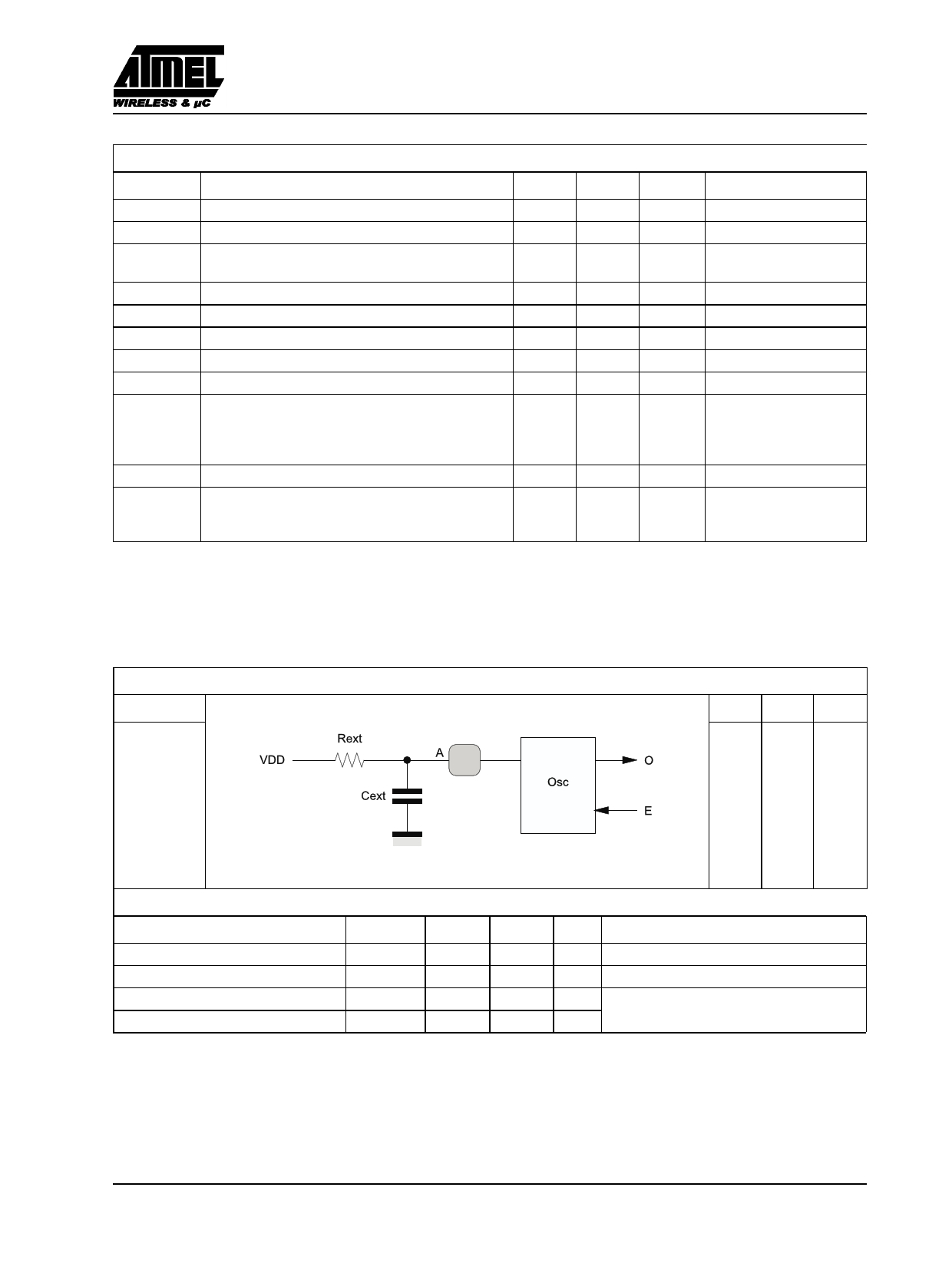
RC 500kHz oscillator (PWDOSC500C5V)
EAO
H500
H X FouT
LLL
LHH
Current consomption
Temperature range
Oscillator frequency range
Cyclic ratio range
AC/DC Characteristics
min typ max unit
400
1200
µA
-40
+125
oC
400 500 600 kHz
40 50 60 %
test conditions
Rext = 8.66kΩ, Cext = 1nF
E = High
Rev. B - June. 07, 2000
11
datasheet pdf - http://www.DataSheet4U.net/
11 Page | ||
| Páginas | Total 16 Páginas | |
| PDF Descargar | [ Datasheet TSS-IO16-E.PDF ] | |
Hoja de datos destacado
| Número de pieza | Descripción | Fabricantes |
| TSS-IO16-E | Van Peripheral Circuit - 16 Inputs-outputs | ATMEL Corporation |
| Número de pieza | Descripción | Fabricantes |
| SLA6805M | High Voltage 3 phase Motor Driver IC. |
Sanken |
| SDC1742 | 12- and 14-Bit Hybrid Synchro / Resolver-to-Digital Converters. |
Analog Devices |
|
DataSheet.es es una pagina web que funciona como un repositorio de manuales o hoja de datos de muchos de los productos más populares, |
| DataSheet.es | 2020 | Privacy Policy | Contacto | Buscar |
