|
|
PDF NCV8870 Data sheet ( Hoja de datos )
| Número de pieza | NCV8870 | |
| Descripción | Automotive Grade Non-Synchronous Boost Controller | |
| Fabricantes | ON Semiconductor | |
| Logotipo | ||
Hay una vista previa y un enlace de descarga de NCV8870 (archivo pdf) en la parte inferior de esta página. Total 15 Páginas | ||
|
No Preview Available !
NCV8870
Automotive Grade
Non-Synchronous Boost
Controller
The NCV8870 is an adjustable output non−synchronous boost
controller which drives an external N-channel MOSFET. The device
uses peak current mode control with internal slope compensation.
The IC incorporates an internal regulator that supplies charge to the
gate driver.
Protection features include internally-set soft-start, undervoltage
lockout, cycle-by-cycle current limiting, hiccup-mode short-circuit
protection and thermal shutdown.
Additional features include low quiescent current sleep mode and
externally-synchronizable switching frequency.
Features
• Peak Current Mode Control with Internal Slope Compensation
• 1.2 V ±2% Reference voltage
• Fixed Frequency Operation
• Wide Input Voltage Range of 3.2 V to 40 Vdc, 45 V Load Dump
• Input Undervoltage Lockout (UVLO)
• Internal Soft-Start
• Low Quiescent Current in Sleep Mode
• Cycle-by-Cycle Current Limit Protection
• Hiccup-Mode Overcurrent Protection (OCP)
• Hiccup-Mode Short-Circuit Protection (SCP)
• Thermal Shutdown (TSD)
• This is a Pb-Free Device
www.onsemi.com
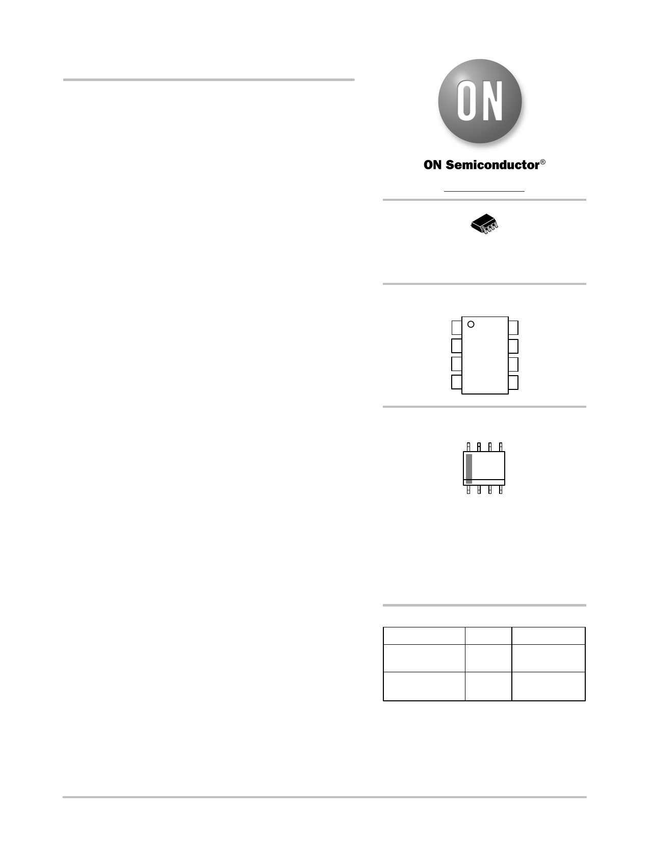
SOIC−8
D SUFFIX
CASE 751
PIN CONNECTIONS
EN/SYNC 1
ISNS 2
GND 3
GDRV 4
8 VFB
7 VC
6 VIN
5 VDRV
MARKING DIAGRAM
8
8870xx
ALYW
G
1
(Top View)
8870xx = Specific Device Code
xx = 00, 01
A = Assembly Location
L = Wafer Lot
Y = Year
W = Work Week
G = Pb−Free Package
ORDERING INFORMATION
Device
Package
NCV887000D1R2G SOIC−8
(Pb−Free)
Shipping†
2500 /
Tape & Reel
NCV887001D1R2G SOIC−8
(Pb−Free)
2500 /
Tape & Reel
†For information on tape and reel specifications,
including part orientation and tape sizes, please
refer to our Tape and Reel Packaging Specification
Brochure, BRD8011/D.
© Semiconductor Components Industries, LLC, 2016
August, 2016 − Rev. 10
1
Publication Order Number:
NCV8870/D
1 page 
NCV8870
ELECTRICAL CHARACTERISTICS (continued)
(−40°C < TJ < 150°C, 3.2 V < VIN < 40 V, unless otherwise specified) Min/Max values are guaranteed by test, design or statistical correlation.
Characteristic
Symbol
Conditions
Min Typ Max Unit
UVLO
Undervoltage Lock-out,
Threshold Voltage
Vuvlo
VIN falling
3.0 3.1 3.2
V
Undervoltage Lock-out,
Hysteresis
Vuvlo,hys
VIN rising
50 125 200 mV
SHORT CIRCUIT PROTECTION
Startup Blanking Period
Hiccup-mode Period
Short Circuit Threshold Voltage
Short Circuit Delay
THERMAL SHUTDOWN
%tscp,dly
%thcp,dly
%Vscp
tscp
From start of soft-start, Percent of tss
From shutdown to start of soft-start,
Percent of tss
VFB as percent of Vref
From VFB < Vscp to stop switching
100 120 150
65 80 95
60 67 75
− 35 100
%
%
%
ns
Thermal Shutdown Threshold
Tsd TJ rising
160 170 180
°C
Thermal Shutdown Hysteresis
Tsd,hys
TJ falling
10 15 20
°C
Thermal Shutdown Delay
tsd,dly
From TJ > Tsd to stop switching
− − 100 ns
Product parametric performance is indicated in the Electrical Characteristics for the listed test conditions, unless otherwise noted. Product
performance may not be indicated by the Electrical Characteristics if operated under different conditions.
www.onsemi.com
5
5 Page 
NCV8870
VIN
VC
R2
C2
C1
RESD
VCTRL
R0
OTA
GDRV
Vd
1:N
Lp
Rds(on)
VOUT
rCf
COUT
ROUT
ISNS
VREF
VFB
Ri
R1
GND
Rlow
Figure 12. NCV8870 Flyback Converter OTA and Compensation
The following equations may be used to select compensation
components R2, C1, C2 for Figures 11 & 12 power supply.
Required input design parameters for analysis are:
Vd = Output diode Vf (V)
VIN = Power supply input voltage (V)
N = Ns/Np (Flyback transformer turns ratio)
Ri = Current sense resistor (W)
RDS(on) = MOSFET RDS(on) (W)
(Rsw_eq = RDS(on) + Ri for the boost continuous conduction
mode (CCM) expressions)
COUT = Bulk output capacitor value (F)
rCF = Bulk output capacitor ESR (W)
ROUT = Equivalent resistance of output load (W)
Pout = Output Power (W)
L = Boost inductor value or flyback transformer primary
side inductance (H)
rL = Boost inductor ESR (W)
Ts = 1/fs, where fs = clock frequency (Hz)
R1 and Rlow = Feedback resistor divider values used to set the
output voltage (W)
VOUT = Device specific output voltage (defined by R1 and
Rlow values) (V)
R0 = OTA output resistance = 3 MW
Sa = IC slope compensation (e.g. 33 mV/ms for NCV887001)
gm = OTA transconductance = 1.2 mS
D = Controller duty ratio
D’ = 1 − D
Necessary equations for describing the modulator gain
(Vctrl-to-Vout gain) Hctrl_output(f) are described next. Boost
continuous conduction mode (CCM) and discontinuous
conduction mode (DCM) transfer function expressions are
summarized in Table 1. Flyback CCM and DCM transfer
function expressions are summarized in Table 2.
www.onsemi.com
11
11 Page | ||
| Páginas | Total 15 Páginas | |
| PDF Descargar | [ Datasheet NCV8870.PDF ] | |
Hoja de datos destacado
| Número de pieza | Descripción | Fabricantes |
| NCV8870 | Automotive Grade Non-Synchronous Boost Controller | ON Semiconductor |
| NCV8871 | Automotive Grade Non-Synchronous Boost Controller | ON Semiconductor |
| NCV887200 | Automotive Grade Non-Synchronous Boost Controller | ON Semiconductor |
| NCV8873 | Automotive Grade Non-Synchronous Boost Controller | ON Semiconductor |
| Número de pieza | Descripción | Fabricantes |
| SLA6805M | High Voltage 3 phase Motor Driver IC. |
Sanken |
| SDC1742 | 12- and 14-Bit Hybrid Synchro / Resolver-to-Digital Converters. |
Analog Devices |
|
DataSheet.es es una pagina web que funciona como un repositorio de manuales o hoja de datos de muchos de los productos más populares, |
| DataSheet.es | 2020 | Privacy Policy | Contacto | Buscar |
