|
|
|
PDF 74LVC1G86 Data sheet ( Hoja de datos )
| Número de pieza | 74LVC1G86 | |
| Descripción | SINGLE 2 INPUT EXCLUSIVE OR GATE | |
| Fabricantes | Diodes | |
| Logotipo | ||
Hay una vista previa y un enlace de descarga de 74LVC1G86 (archivo pdf) en la parte inferior de esta página. Total 12 Páginas | ||
|
No Preview Available !
74LVC1G86
SINGLE 2 INPUT EXCLUSIVE OR GATE
Description
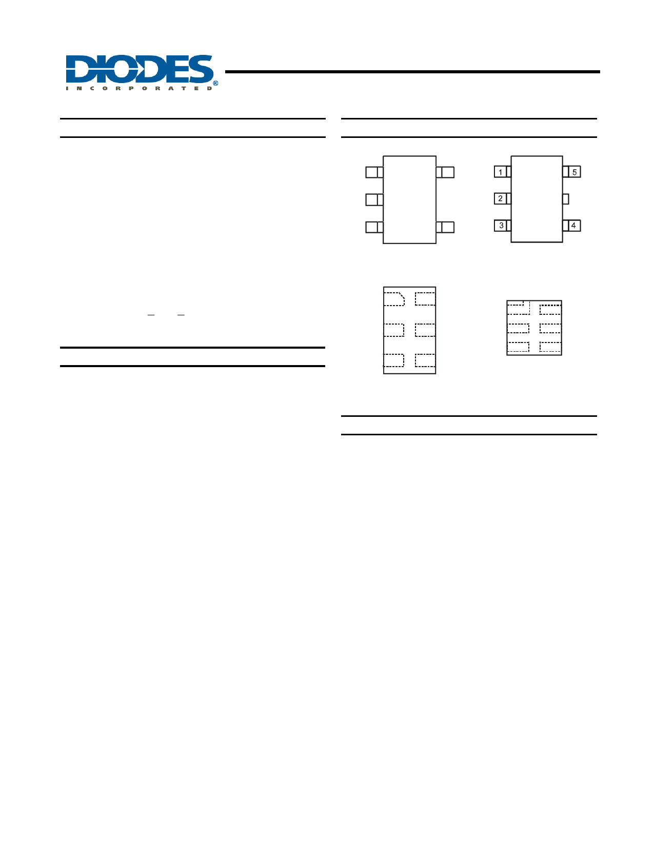
Pin Assignments
The 74LVC1G86 is a single 2-input EXCLUSIVE OR gate
( Top View )
(Top View)
with a standard push-pull output. The device is designed for
operation with a power supply range of 1.65V to 5.5V. The
inputs are tolerant to 5.5V allowing this device to be used in a
A1
B2
5 VCC A
B
VCC
mixed voltage environment. The device is fully specified for
partial power down applications using IOFF. The IOFF circuitry
disables the output preventing damaging current backflow
when the device is powered down.
The gate performs the positive Boolean function:
Y = A ⊕ B or Y = AB + AB
Features
• Wide Supply Voltage Range from 1.65 to 5.5V
• ± 24mA Output Drive at 3.3V
• CMOS low power consumption
• IOFF Supports Partial-Power-Down Mode Operation
• Inputs accept up to 5.5V
• ESD Protection Tested per JESD 22
o Exceeds 200-V Machine Model (A115-A)
o Exceeds 2000-V Human Body Model (A114-A)
o Exceeds 1000-V Charged Device Model (C101C)
• Latch-Up Exceeds 100mA per JESD 78, Class II
• Range of Package Options
• Direct Interface with TTL Levels
• All packages Assembled with “Green” Molding
Compound (no Br, Sb)
• Lead Free Finish/ RoHS Compliant (Note 1)
GND 3
4 Y GND
Y
SOT25 / SOT353
(Top View)
A1
6 VCC
B2
5 NC
GND 3
4Y
X2-DFN1410-6
SOT553
Top View
(Top View)
A1
6 VCC
B2
5 NC
GND 3
4Y
X2-DFN1010-6
Applications
• Voltage Level Shifting
• Bus Driver / Repeater
• Parity Bit Generation
• Selectable signal Inverter
• Power Down Signal Isolation
• General Purpose Logic
• Wide array of products such as:
o PCs, networking, notebooks, netbooks, PDAs
o Tablet Computers, E-readers
o Computer peripherals, hard drives, CD/DVD ROM
o TV, DVD, DVR, set top box
o Cell Phones, Personal Navigation / GPS
o MP3 players ,Cameras, Video Recorders
Notes:
1. EU Directive 2002/95/EC (RoHS) & 2011/65/EU (RoHS 2) compliant. No purposely added lead. Halogen and Antimony free.
Please visit our website at http://www.diodes.com/products/lead_free.html
74LVC1G86
Document number: DS32201 Rev. 6 - 2
1 of 12
www.diodes.com
February 2012
© Diodes Incorporated
Free Datasheet http://www.datasheet4u.com/
1 page 
74LVC1G86
SINGLE 2 INPUT EXCLUSIVE OR GATE
Package Characteristics (All typical values are at VCC = 3.3V, TA = 25°C)
Symbol
Parameter
θJA
Thermal Resistance
Junction-to-Ambient
θJC
Thermal Resistance
Junction-to-Case
Test Conditions
SOT25
SOT353
SOT553
X2-DFN1010-6
X2-DFN1410-6
SOT25
SOT353
SOT553
X2-DFN1010-6
X2-DFN1410-6
VCC
(Note 4)
(Note 4)
Min Typ. Max Unit
204
371 oC/W
231
445
460
52
143 oC/W
105
250
265
Notes: 4. Test condition for SOT25, SOT353, SOT553, X2-DFN1410-6 and X2-DFN1010-6: Device mounted on FR-4 substrate PC board, 2oz copper, with
minimum recommended pad layout.
Switching Characteristics
Figure 1 Typical Values at TA = 25 ºC and nominal voltages 1.8V, 2.5V, 2.7V, 3.3V, and 5.0V.
Parameter
From
Input
To
Output
VCC
TA = -40ºC to 85ºC
Min Typ. Max
TA = -40ºC to 125ºC
Min Max
1.8V ± 0.15V
1.0
3.7
9.9
1.0 13.0
2.5V ± 0.2V
0.5
2.5
5.5
0.5
7.0
tpd A or B Y
2.7V
0.5 2.8 5.8 0.5
7.5
3.3V ± 0.3V
0.5
2.3
5.0
0.5
6.5
5.0V ± 0.5V
0.5
1.9
4.0
0.5
5.5
Unit
ns
Operating Characteristics
TA = 25ºC
Parameter
Power dissipation
Cpd capacitance
Test
Conditions
f = 10 MHz
VCC = 1.8V
Typ.
14
VCC = 2.5V
Typ.
14
VCC = 3.3V
Typ.
14
VCC = 5V
Typ.
14
Unit
pF
74LVC1G86
Document number: DS32201 Rev. 6 - 2
5 of 12
www.diodes.com
February 2012
© Diodes Incorporated
5 Page 
Suggested Pad Layout (cont.)
(4) Package Type X2-DFN1010-6
X1
C
Y1
1
G(4x)
74LVC1G86
SINGLE 2 INPUT EXCLUSIVE OR GATE
Y (6x)
X(6x)
Dimensions
C
G
X
X1
Y
Y1
Value
(in mm)
0.350
0.150
0.200
0.900
0.550
1.250
(5) Package Type: X2-DFN1410-6
X1
C
Y1
Y(6x)
1
G(4x)
X(6x)
Dimensions
C
G
X
X1
Y
Y1
Value
(in mm)
0.500
0.250
0.250
1.250
0.525
1.250
74LVC1G86
Document number: DS32201 Rev. 6 - 2
11 of 12
www.diodes.com
February 2012
© Diodes Incorporated
11 Page | ||
| Páginas | Total 12 Páginas | |
| PDF Descargar | [ Datasheet 74LVC1G86.PDF ] | |
Hoja de datos destacado
| Número de pieza | Descripción | Fabricantes |
| 74LVC1G80 | Single D-type flip-flop; positive-edge trigger | Panasonic Semiconductor |
| 74LVC1G80GM | Single D-type flip-flop; positive-edge trigger | Panasonic Semiconductor |
| 74LVC1G80GV | Single D-type flip-flop; positive-edge trigger | Panasonic Semiconductor |
| 74LVC1G80GW | Single D-type flip-flop; positive-edge trigger | Panasonic Semiconductor |
| Número de pieza | Descripción | Fabricantes |
| SLA6805M | High Voltage 3 phase Motor Driver IC. |
Sanken |
| SDC1742 | 12- and 14-Bit Hybrid Synchro / Resolver-to-Digital Converters. |
Analog Devices |
|
DataSheet.es es una pagina web que funciona como un repositorio de manuales o hoja de datos de muchos de los productos más populares, |
| DataSheet.es | 2020 | Privacy Policy | Contacto | Buscar |