|
|
|
PDF NOIL1SM4000A Data sheet ( Hoja de datos )
| Número de pieza | NOIL1SM4000A | |
| Descripción | 4 MegaPixel High Speed CMOS Sensor | |
| Fabricantes | ON Semiconductor | |
| Logotipo | ||
Hay una vista previa y un enlace de descarga de NOIL1SM4000A (archivo pdf) en la parte inferior de esta página. Total 30 Páginas | ||
|
No Preview Available !
NOIL1SM4000A
LUPA4000: 4 MegaPixel
High Speed CMOS Sensor
Features
• 2048 x 2048 Active Pixels
• 12 mm x 12 mm Square Pixels
• 24.6 mm x 24.6 mm Optical Format
• Monochrome or Color Digital Output
• 15 Frames per Second (fps) at Full Resolution
• Pipelined Global Shutter
• Random Programmable Region of Interest (ROI) Readout and
Subsampling Modes
• Serial Peripheral Interface (SPI)
• Operational Range: 0°C to 60°C
• 127-Pin PGA Package
• 220 mW Power Dissipation
• These Devices are Pb−Free and are RoHS Compliant
http://onsemi.com
Applications
• Intelligent Traffic System
• High Speed Machine Vision
Overview
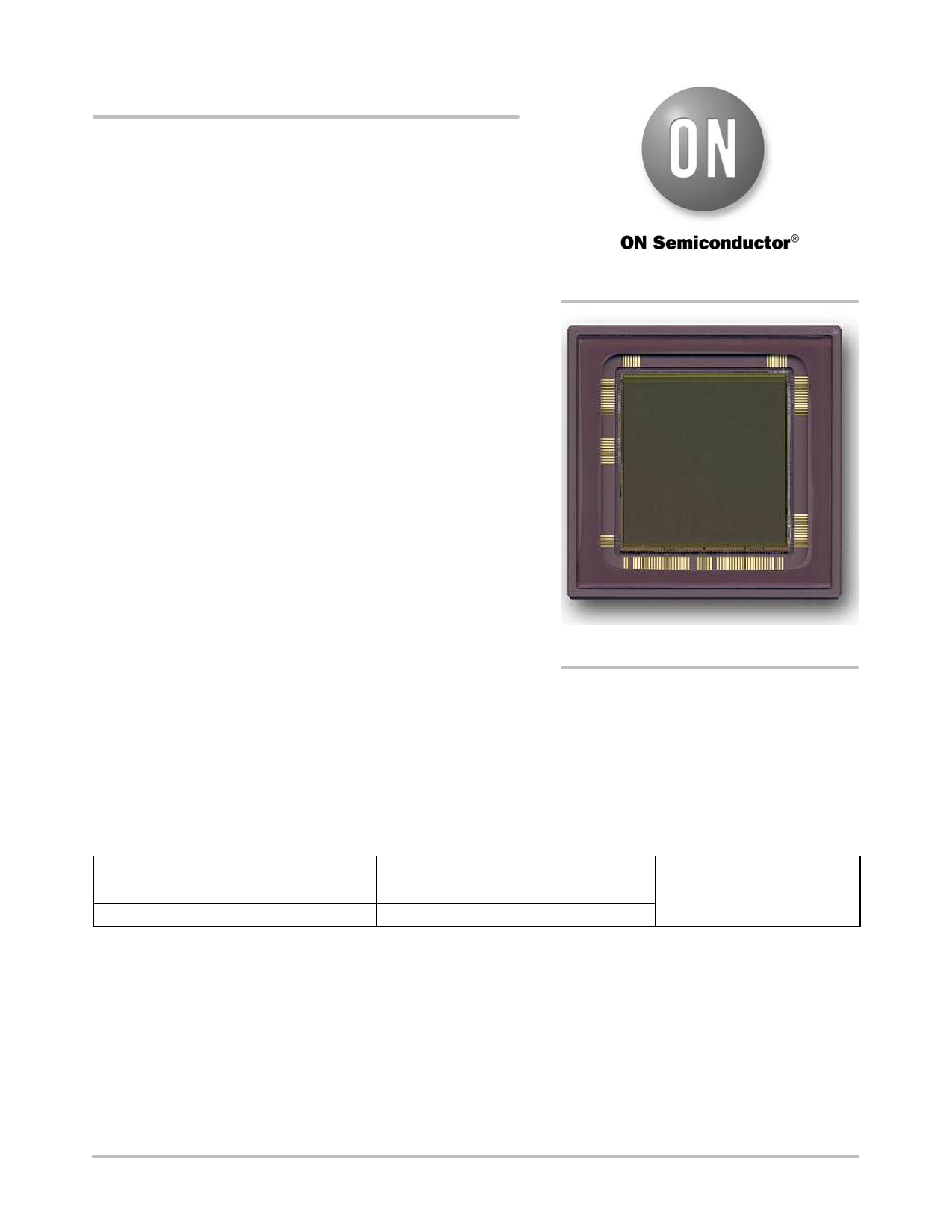
Figure 1. LUPA4000 Photo
The LUPA4000 is a CMOS image sensor (CIS) with a 4.0
megapixel resolution 2048 x 2048 pixel format.
This document describes the interfacing and driving of the LUPA4000 image sensor. This 4 megapixel CMOS active pixel
sensor features synchronous shutter and a maximal frame rate of 15 fps in full resolution. The readout speed can be boosted
by sub-sampling and windowed ROI readout. High dynamic range scenes can be captured using the double and multiple
slope functionality.
The sensor uses a 3-wire SPI and is housed in a 127-pin ceramic PGA package. The LUPA4000 is available in mono and
color option.
ORDERING INFORMATION
Marketing Part Number
NOIL1SM4000A-GDC
NOIL1SC4000A-GDC
Description
Mono with Glass
Color with Glass
NOTE: Refer to Ordering Code Definition on page 26 for more information.
Package
127−pin PGA
© Semiconductor Components Industries, LLC, 2013
February, 2013 − Rev. 9
1
Publication Order Number:
NOIL1SM4000A/D
Free Datasheet http://www.datasheet4u.com/
1 page 
NOIL1SM4000A
OVERVIEW
The LUPA4000 CMOS active pixel sensor features a
global shutter with a maximum frame rate of 15 fps in full
resolution. The readout speed is boosted by sub sampling
and the windowed ROI readout. High dynamic range scenes
can be captured using the multiple slope functionality.
Subsampling reduces resolution while maintaining the
constant field of view and an increased frame rate.
The sensor uses a 3-wire SPI. It requires only one master
clock for operation up to 15 fps. The sensor is available in
a monochrome version or Bayer (RGB) patterned color filter
array. It is placed in a 127-pin ceramic PGA package.
Color Filter Array
The color version of LUPA4000 is available in Bayer
(RGB) patterned color filter array. The orientation of RGB
is shown in Figure 2.
The spectral response for the mono and color device is
shown in Figure 3.
LUPA4000
Pixel Array
G
(0.1)
R
(0.0)
B
(1.1)
G
(1.0)
x_readout direction
Figure 2. Color Filter Array
Figure 3. Spectral Response Curve for Mono and Color
http://onsemi.com
5
Free Datasheet http://www.datasheet4u.com/
5 Page 
NOIL1SM4000A
Figure 11. Internal Timing of Pixel
In Figure 11, levels are defined by the pixel array voltage
supplies; for correct polarities of the signals see Table 4. The
signals in Figure 11 are generated from the on-chip drivers.
These on-chip drivers need two types of signals to generate
the exact type of signal. It needs digital control signals
between 0 V and 3.3 V (internally converted to 2.5 V) with
normal driving capability and power supplies. The control
signals are required to indicate when they must occur and the
power supplies indicate the level.
Vmem is made of a control signal Mem_hl and 2 supplies
Vmem_h and Vmem_l. If the signal Mem_hl is the logic ‘0’
than the internal signal Vmem is low, if Mem_hl is logic ‘1’
the internal signal Vmem is high.
Reset is made with two control signals, Reset and
Reset_ds, and two supplies, Vres and Vres_ds. Depending
on the signal that becomes active, the corresponding supply
level is applied to the pixel.
Table 4 summarizes the relation between the internal and
external pixel array signals.
Table 4. OVERVIEW OF INTERNAL AND EXTERNAL PIXEL ARRAY SIGNALS
Internal Signal
Vlow
Vhigh
External Control Signal
Precharge
0 0.45 V
Precharge (AL)
Sample
Reset
Vmem
0
0
2.0 V to 2.5 V
2.5 V
2.5 V to 3.3 V
2.5 V to 3.3 V
Sample (AL)
Reset (AH) and Reset_ds (AH)
Mem_hl (AL)
Low DC Level
Vpre_l
Gnd
Gnd
Vmem_l
High DC Level
Controlled by
bias-resistor
Vdd
Vres and Vres_ds
Vmem_h
For dual slope operation, give a second reset pulse to a
lower reset level during integration. This is done by the
control signal Reset_ds and by the power supply Vres_ds
that defines the level to which the pixel must be reset.
Note that Reset is dominant over Reset_ds, which means
that the high voltage level is applied for reset, if both pulses
occur at the same time.
Multiple slopes are possible having multiple Reset_ds
pulses with a lower Vres_ds level for each pulse given within
the same integration time.
The rise and fall times of the internal generated signals are
not very fast (200 ns). In fact they are made rather slow to
limit the maximum current through the power supply lines
(Vmem_h, Vmem_l, Vres, Vres_ds, Vdd). Current
limitation of those power supplies is not required. However,
limit the currents to not higher than 400 mA.
The power supply Vmem_l must be able to sink this
current because it must be able to discharge the internal
capacitance from the level Vmem_h to the level Vmem_l.
The external control signals should be capable of driving
input capacitance of about 10 pF.
Digital Signals
The digital signals control the readout of the image sensor.
These signals are:
• Sync_y (AH[10]): Starts the readout of the frame. This
pulse synchronises the y-address register: active high.
This signal is also the end of the frame or window and
determines the window width.
• Clock_y (AH[10]): Clock of the y-register. On the rising
edge of this clock, the next line is selected.
• Sync_x (AH[10]): Starts the readout of the selected line
at the address defined by the x-address register. This
pulse synchronises the x-address register: active high.
This signal is also the end of the line and determines the
window length.
• Clock_x (AH[10]): Determines the pixel rate. A clock of
33 MHz is required to achieve a pixel rate of 66 MHz.
• Spi_data (AH[10]): Data for the SPI.
• Spi_clock (AH[10]): Clock of the SPI. This clock
downloads the data into the SPI register.
http://onsemi.com
11
Free Datasheet http://www.datasheet4u.com/
11 Page | ||
| Páginas | Total 30 Páginas | |
| PDF Descargar | [ Datasheet NOIL1SM4000A.PDF ] | |
Hoja de datos destacado
| Número de pieza | Descripción | Fabricantes |
| NOIL1SM4000A | 4 MegaPixel High Speed CMOS Sensor | ON Semiconductor |
| Número de pieza | Descripción | Fabricantes |
| SLA6805M | High Voltage 3 phase Motor Driver IC. |
Sanken |
| SDC1742 | 12- and 14-Bit Hybrid Synchro / Resolver-to-Digital Converters. |
Analog Devices |
|
DataSheet.es es una pagina web que funciona como un repositorio de manuales o hoja de datos de muchos de los productos más populares, |
| DataSheet.es | 2020 | Privacy Policy | Contacto | Buscar |