|
|
|
PDF AD9119 Data sheet ( Hoja de datos )
| Número de pieza | AD9119 | |
| Descripción | (AD9119 / AD9129) RF Digital-to-Analog Converter | |
| Fabricantes | Analog Devices | |
| Logotipo | ||
Hay una vista previa y un enlace de descarga de AD9119 (archivo pdf) en la parte inferior de esta página. Total 68 Páginas | ||
|
No Preview Available !
Data Sheet
FEATURES
DAC update rate: up to 5.6 GSPS
Direct RF synthesis at 2.8 GSPS data rate
DC to 1.4 GHz in baseband mode
DC to 1.0 GHz in 2× interpolation mode
1.4 GHz to 4.2 GHz in Mix-Mode
Bypassable 2× interpolation
Excellent dynamic performance
Supports DOCSIS 3.0 wideband ACLR/harmonic performance
8 QAM carriers: ACLR > 65 dBc
Industry-leading single/multicarrier IF or RF synthesis
4-carrier W-CDMA ACLR at 2457.6 MSPS
fOUT = 900 MHz, ACLR = 71 dBc (baseband mode)
fOUT = 2100 MHz, ACLR = 68 dBc (Mix-Mode)
fOUT = 2700 MHz, ACLR = 67 dBc (Mix-Mode)
Dual-port LVDS and DHSTL data interface
Up to 1.4 GSPS operation
Source synchronous DDR clocking with parity bit
Low power: 1.0 W at 2.8 GSPS (1.3 W at 5.6 GSPS)
APPLICATIONS
Broadband communications systems
CMTS/VOD
Wireless infrastructure: W-CDMA, LTE, point-to-point
Instrumentation, automatic test equipment (ATE)
Radars, jammers
GENERAL DESCRIPTION
The AD9119/AD9129 are high performance, 11-/14-bit RF digital-
to-analog converters (DACs) supporting data rates up to 2.8 GSPS.
The DAC core is based on a quad-switch architecture that enables
dual-edge clocking operation, effectively increasing the DAC
update rate to 5.6 GSPS when configured for Mix-Mode™ or 2×
interpolation. The high dynamic range and bandwidth enable
multicarrier generation up to 4.2 GHz.
In baseband mode, wide bandwidth capability combines with high
dynamic range to support from 1 to 158 contiguous carriers for
CATV infrastructure applications. A choice of two optional 2×
interpolation filters is available to simplify the postreconstruction
filter by effectively increasing the DAC update rate by a factor of 2.
In Mix-Mode operation, the AD9119/AD9129 can reconstruct
RF carriers in the second and third Nyquist zone while still
maintaining exceptional dynamic range up to 4.2 GHz. The
high performance NMOS DAC core features a quad-switch
architecture that enables industry-leading direct RF synthesis
performance with minimal loss in output power. The output
current can be programmed over a range of 9.5 mA to 34.4 mA.
Rev. 0
Document Feedback
Information furnished by Analog Devices is believed to be accurate and reliable. However, no
responsibilityisassumedbyAnalogDevices for itsuse,nor foranyinfringementsofpatentsor other
rights of third parties that may result from its use. Specifications subject to change without notice. No
license is granted by implication or otherwise under any patent or patent rights of Analog Devices.
Trademarksandregisteredtrademarksarethepropertyoftheirrespectiveowners.
11-/14-Bit, 5.6 GSPS,
RF Digital-to-Analog Converter
AD9119/AD9129
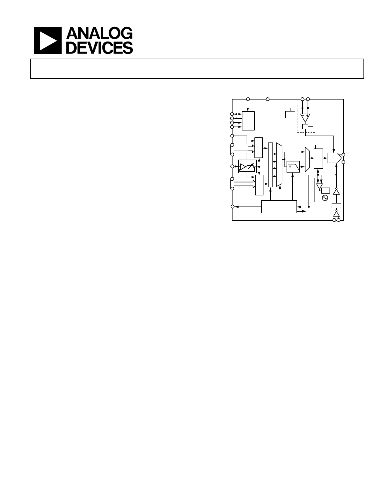
FUNCTIONAL BLOCK DIAGRAM
RESET
IRQ
I250U VREF
SDIO
SDO
CS
SCLK
FRM_x
(FRAME/
PARITY)
P0_D[13:0]P,
P0_D[13:0]N
DCI_x
SPI
DLL
AD9129
1.2V
MIX-
NORMAL MODE
BASEBAND
MODE
Tx DAC
CORE
2×
IOUTP
IOUTN
P1_D[13:0]P,
P1_D[13:0]N
PLL
DCO_x
CLOCK
DISTRIBUTION
Figure 1.
DCR
DACCLK_x
The AD9119/AD9129 include several features that may further
simplify system integration. A dual-port, source synchronous
LVDS interface simplifies the data interface to a host FPGA/ASIC.
A differential frame/parity bit is also included to monitor the
integrity of the interface. On-chip delay locked loops (DLLs)
are used to optimize timing between different clock domains.
A serial peripheral interface (SPI) is used to configure the
AD9119/AD9129 and monitor the status of readback registers.
The AD9119/AD9129 is manufactured on a 0.18 µm CMOS
process and operates from +1.8 V and −1.5 V supplies. It is
supplied in a 160-ball chip scale package ball grid array.
PRODUCT HIGHLIGHTS
1. High dynamic range and signal reconstruction bandwidth
support RF signal synthesis of up to 4.2 GHz.
2. Dual-port interface with double data rate (DDR) LVDS
data receivers supports 2800 MSPS maximum conversion rate.
3. Manufactured on a CMOS process; a proprietary switching
technique enhances dynamic performance.
One Technology Way, P.O. Box 9106, Norwood, MA 02062-9106, U.S.A.
Tel: 781.329.4700
©2013 Analog Devices, Inc. All rights reserved.
Technical Support
www.analog.com
Free Datasheet http://www.datasheet4u.com/
1 page 
Data Sheet
SERIAL PORT AND CMOS PIN SPECIFICATIONS
VDDA = VDD = 1.8 V, VSSA = −1.5 V, IOUTFS = 33 mA, TA = −40°C to +85°C.
Table 4.
Parameter
WRITE OPERATION
SCLK Clock Rate
SCLK Clock High
SCLK Clock Low
SDIO to SCLK Setup Time
SCLK to SDIO Hold Time
CS to SCLK Setup Time
SCLK to CS Hold Time
READ OPERATION
SCLK Clock Rate
SCLK Clock High
SCLK Clock Low
SDIO to SCLK Setup Time
SCLK to SDIO Hold Time
CS to SCLK Setup Time
SCLK to SDIO (or SDO) Data Valid Time
CS to SDIO (or SDO) Output Valid to High-Z
INPUTS (SDI, SDIO, SCLK, CS)
Voltage In High
Voltage In Low
Current In High
Current In Low
OUTPUTS (SDIO, SYNC)
Voltage Out High
Voltage Out Low
Current Out High
Current Out Low
Symbol
fSCLK, 1/tSCLK
tHIGH
tLOW
tDS
tDH
tS
tH
fSCLK, 1/tSCLK
tHIGH
tLOW
tDS
tDH
tS
tDV
tEZ
VIH
VIL
IIH
IIL
VOH
VOL
IOH
IOL
Test Comments/Conditions
See Figure 126
See Figure 127
Min
20
20
10
5
10
5
20
20
10
5
10
1.2
−150
1.3
0
AD9119/AD9129
Typ Max Unit
20 MHz
ns
ns
ns
ns
ns
ns
20 MHz
ns
ns
ns
ns
ns
10 ns
2
1.8 V
0 0.4 V
+75 µA
µA
2.0 V
0.3 V
4 mA
4 mA
Rev. 0 | Page 5 of 68
Free Datasheet http://www.datasheet4u.com/
5 Page 
Data Sheet
AD9119/AD9129
Pin No.
A12, A13, A14, B12, B13, C11,
C12, D5, D6, D8, D9, D10, D11,
E3, E4, F1, F2, F3, F4, G4
A6
A7
B14
C1, D1
H1
H2
J1
J2
K1
K2
K3, K4
K11, K12
K13, K14
L1, M1
L2, M2
L3, M3
L4, M4
L5, M5
L6, M6
L7, M7
L8, M8
L9, M9
L10, M10
L11, M11
L12,M12
L13, M13
L14, M14
N1, P1
N2, P2
N3, P3
N4, P4
N5, P5
N6, P6
N7, P7
N8, P8
N9, P9
N10, P10
N11, P11
N12, P12
N13, P13
N14, P14
Mnemonic
VSSC
Description
Analog Supply Return.
IOUTP
IOUTN
SYNC
DACCLK_N, DACCLK_P
RESET
IRQ
SDIO
SDO
SCLK
CS
DCI_P, DCI_N
DCO_P, DCO_N
FRM_P, FRM_N
P1_D0P, P1_D0N
P1_D1P, P1_D1N
P1_D2P, P1_D2N
P1_D3P, P1_D3N
P1_D4P, P1_D4N
P1_D5P, P1_D5N
P1_D6P, P1_D6N
P1_D7P, P1_D7N
P1_D8P, P1_D8N
P1_D9P, P1_D9N
P1_D10P, P1_D10N
P1_D11P, P1_D11N
P1_D12P, P1_D12N
P1_D13P, P1_D13N
P0_D0P, P0_D0N
P0_D1P, P0_D1N
P0_D2P, P0_D2N
P0_D3P, P0_D3N
P0_D4P, P0_D4N
P0_D5P, P0_D5N
P0_D6P, P0_D6N
P0_D7P, P0_D7N
P0_D8P, P0_D8N
P0_D9P, P0_D9N
P0_D10P, P0_D10N
P0_D11P, P0_D11N
P0_D12P, P0_D12N
P0_D13P, P0_D13N
DAC Positive Current Output Source.
DAC Negative Current Output Source.
Synchronization Signal Output.
Negative/Positive DAC Clock Input.
Reset Input. Active high. If unused, tie this pin to VSS.
Interrupt Request Open-Drain Output. Active high. Pull up this pin to VDD
with a 1 kΩ resistor.
Serial Port Data Input/Output.
Serial Port Data Output.
Serial Port Clock Input.
Serial Port Enable Input.
Positive, Negative Data Clock Input (DCI).
Positive, Negative Data Clock Output (DCO).
Positive, Negative Data Frame/Parity Signal (FRAME/PARITY).
Data Port 1 Positive/Negative Data Input Bit 0.
Data Port 1 Positive/Negative Data Input Bit 1.
Data Port 1 Positive/Negative Data Input Bit 2.
Data Port 1 Positive/Negative Data Input Bit 3.
Data Port 1 Positive/Negative Data Input Bit 4.
Data Port 1 Positive/Negative Data Input Bit 5.
Data Port 1 Positive/Negative Data Input Bit 6.
Data Port 1 Positive/Negative Data Input Bit 7.
Data Port 1 Positive/Negative Data Input Bit 8.
Data Port 1 Positive/Negative Data Input Bit 9.
Data Port 1 Positive/Negative Data Input Bit 10.
Data Port 1 Positive/Negative Data Input Bit 11.
Data Port 1 Positive/Negative Data Input Bit 12.
Data Port 1 Positive/Negative Data Input Bit 13.
Data Port 0 Positive/Negative Data Input Bit 0.
Data Port 0 Positive/Negative Data Input Bit 1.
Data Port 0 Positive/Negative Data Input Bit 2.
Data Port 0 Positive/Negative Data Input Bit 3.
Data Port 0 Positive/Negative Data Input Bit 4.
Data Port 0 Positive/Negative Data Input Bit 5.
Data Port 0 Positive/Negative Data Input Bit 6.
Data Port 0 Positive/Negative Data Input Bit 7.
Data Port 0 Positive/Negative Data Input Bit 8.
Data Port 0 Positive/Negative Data Input Bit 9.
Data Port 0 Positive/Negative Data Input Bit 10.
Data Port 0 Positive/Negative Data Input Bit 11.
Data Port 0 Positive/Negative Data Input Bit 12.
Data Port 0 Positive/Negative Data Input Bit 13.
Rev. 0 | Page 11 of 68
Free Datasheet http://www.datasheet4u.com/
11 Page | ||
| Páginas | Total 68 Páginas | |
| PDF Descargar | [ Datasheet AD9119.PDF ] | |
Hoja de datos destacado
| Número de pieza | Descripción | Fabricantes |
| AD9114 | 8-/10-/12-/14-Bit Low Power Digital-to-Analog Converters | Analog Devices |
| AD9115 | 8-/10-/12-/14-Bit Low Power Digital-to-Analog Converters | Analog Devices |
| AD9116 | 8-/10-/12-/14-Bit Low Power Digital-to-Analog Converters | Analog Devices |
| AD9117 | 8-/10-/12-/14-Bit Low Power Digital-to-Analog Converters | Analog Devices |
| Número de pieza | Descripción | Fabricantes |
| SLA6805M | High Voltage 3 phase Motor Driver IC. |
Sanken |
| SDC1742 | 12- and 14-Bit Hybrid Synchro / Resolver-to-Digital Converters. |
Analog Devices |
|
DataSheet.es es una pagina web que funciona como un repositorio de manuales o hoja de datos de muchos de los productos más populares, |
| DataSheet.es | 2020 | Privacy Policy | Contacto | Buscar |