|
|
|
PDF HIP7010 Data sheet ( Hoja de datos )
| Número de pieza | HIP7010 | |
| Descripción | J1850 Byte Level Interface Circuit | |
| Fabricantes | Intersil Corporation | |
| Logotipo | ||
Hay una vista previa y un enlace de descarga de HIP7010 (archivo pdf) en la parte inferior de esta página. Total 20 Páginas | ||
|
No Preview Available !
HIP7010
ADVANCE INFORMATION
August 1996
J1850 Byte Level Interface Circuit
Features
• Fully Supports VPW (Variable Pulse Width) Messaging
Practices of SAE J1850 Standard for Class B Data
Communications Network Interface
- 3-Wire, High-Speed, Synchronous, Serial Interface
• Reduces Wiring Overhead
• Directly Interfaces with 68HC05 and 68HC11 Style SPI
Ports
• 1MHz, 8-Bit Transfers Between Host and HIP7010
Minimize Host Service Requirements
• Automatically Transmits Properly Framed Messages
• Prepends SOF to First Byte and Appends CRC to Last
Byte
• Fail-Safe Design Including, Slow Clock Detection
Circuitry, Prevents J1850 Bus Lockup Due to System
Errors or Loss of Input Clock
• Automatic Collision Detection
• End of Data (EOD), Break, Idle Bus, and Invalid Symbol
(Noise/Illegal Symbols) Detection
• Supports In-Frame Responses with Generation of
Normalization Bits (NB) for Type 1, Type 2, and Type 3
Messages
• Wait-For-Idle Mode Reduces Host Overhead During
Non-Applicable Messages
• Status Register Flags Provide Information on Current
Status of J1850 Bus
• Serial I/O Pins are Active Only During Transfers - Bus
Available for Other Devices 95% of the Time
• TEST Pin Provides Built-in-Test Capabilities for
In-System Diagnostics and Factory Testing
• High Speed (4X) Receive Mode for Production and
Diagnostic Testing/Programming
• Operates with Wide Range of Input Clock Frequencies
• Power-Saving Power-Down Mode
• Full -40oC to +125oC Operating Range
• Single 3.0V to 6.0V Supply
Description
The Intersil HIP7010, J1850 Byte Level Interface Circuit, is a
member of the Intersil family of low-cost multiplexed wiring
ICs. The integrated functions of the HIP7010 provide the
system designer with components key to building a “Class B”
multiplexed communications network interface, which fully
conforms to the VPW Multiplexed Wiring protocol specified
in the SAE J1850 Standard. The HIP7010 is designed to
interface with a wide variety of Host microcontrollers via a
standard three wire, high-speed (1MHz), synchronous, serial
interface. The HIP7010 automatically produces properly
framed VPW messages, prepending the Start of Frame
(SOF) symbol and calculating and appending the CRC
check byte. All circuitry needed to decode incoming mes-
sages, to validate CRC bytes, and to detect Breaks, End of
Data (EOD), Idle bus, and illegal symbols is included. In-
Frame Responses (IFRs) are fully supported for Type 1,
Type 2, and Type 3 messages, with the appropriate Normal-
ization Bit automatically generated. The HCMOS design
allows proper opeSration at various input frequencies from
2MHz to 12MHz. Connection to the J1850 Bus is via a Inter-
sil HIP7020.
Ordering Information
TEMP.
PART NUMBER RANGE (oC)
PACKAGE
PKG. NO.
HIP7010P
-40 +125 14 Lead Plastic DIP
E14.3
HIP7010B
-40 +125 14 Lead Plastic SOIC (N) M14.15
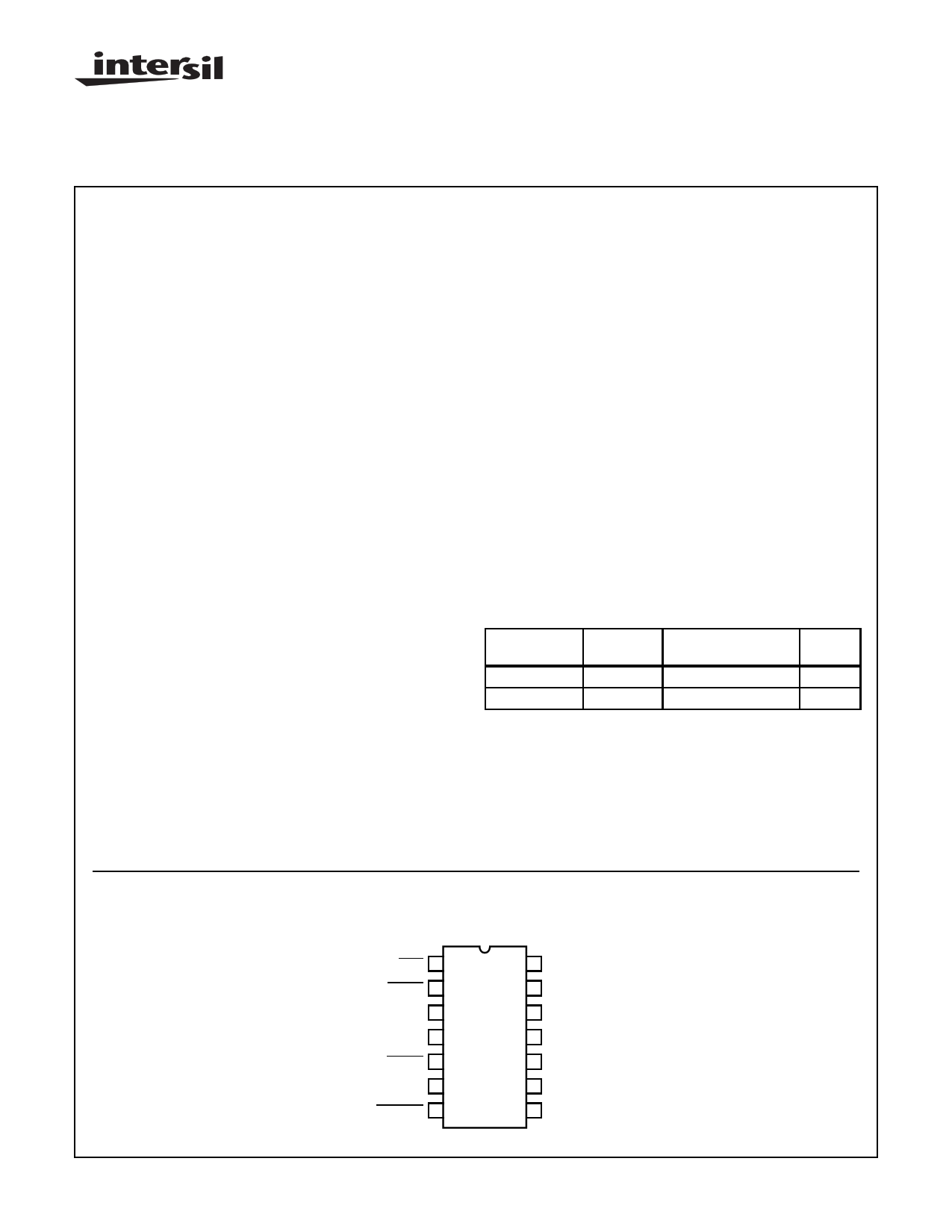
Pinout
HIP7010 (SOIC, PDIP)
TOP VIEW
IDLE 1
VPWIN 2
VPWOUT 3
VDD 4
RESET 5
TEST 6
SACTIVE 7
14 RDY
13 STAT
12 CLK
11 VSS
10 SIN
9 SOUT
8 SCK
CAUTION: These devices are sensitive to electrostatic discharge; follow proper IC Handling Procedures.
www.intersil.com or 407-727-9207 | Copyright © Intersil Corporation 1999
1
File Number 3644.2
1 page 
HIP7010
STAT
(INPUT)
RDY (SHORT)
(INPUT)
(14)
(15)
RDY (LONG)
(INPUT)
SACTIVE
(OUTPUT)
(16)
(17) (18) (19)
(2) (1) (13)
(12) (3)
SCK
(OUTPUT)
SOUT
(OUTPUT)
SIN
(INPUT)
(4) (5)
D7O
(8) (10) (11)
D7I
(6) (7)
D6O
D6I
D0O
(9)
D0I
NOTES:
FIGURE 1. SERIAL INTERFACE TIMING DIAGRAM
1. Measurement points are from VDD/2, except 12 and 13 which are measured between VIL and VIH.
2. All timings assume proper CLK frequency and Divide Select values to generate 1MHz SCK.
Functional Pin Description
This section provides a description of each of the 14 pins of
the HIP7010 as shown in Figure 2.
IDLE 1
VPWIN 2
VPWOUT 3
VDD 4
RESET 5
TEST 6
SACTIVE 7
14 RDY
13 STAT
12 CLK
11 VSS
10 SIN
9 SOUT
8 SCK
FIGURE 2. 14 PIN DIP AND SO TERMINAL ASSIGNMENTS
VDD and VSS (Power)
Power is supplied to the HIP7010 using these two pins. VDD
is connected to the positive supply and VSS is connected to
the negative supply.
CLK (Clock - Input)
The Clock input (CLK) provides the basic time base refer-
ence for all J1850 symbol detection and generation. Serial
Bus transfers between the HIP7010 and the Host microcon-
troller are also timed based on the Clock input. Proper VPW
symbol detection and generation requires a 2MHz clock
which is internally derived from the CLK input. Various CLK
input frequencies can be accommodated via the Divide
Select bits in the Status/Control Register (see Status/Con-
trol Register for details).
An internal Slow Clock Detect circuit monitors the CLK input
signal and generates a HIP7010 reset if the clock is inactive
for more than 1/fSLOW. This is a safety mechanism to prevent
blocking the J1850 and Serial busses in the event of a clock
failure. The Slow Clock Detect reset can also be intentionally
invoked by externally inhibiting CLK input transitions.
Power can be reduced under Host control via the PowerDown
bit in the Status/Control Register (see Status/Control Regis-
ter for details). Setting the Power-Down bit effectively stops
internal clocking of the HIP7010.
5
5 Page 
HIP7010
SERIAL Bus Transfers
The HIP7010 is always configured as a SERIAL “master”. As
a master, the HIP7010 generates the transfer-synchronizing
clock on the SCK pin, transmits data on the SOUT pin, and
receives data on the SIN pin.
Whenever the HIP7010 receives a complete byte from the
J1850 bus via the VPWIN line, it automatically initiates an
unsolicited SERIAL transfer. The unsolicited transfer trans-
mits the received (or reflected) byte to the Host and, if in the
midst of transmitting a message, retrieves the next byte from
the Host. While these unsolicited transfers are, strictly
speaking, asynchronous to the Host’s activities, there are
well defined rules which govern the minimum time between
unsolicited transfers (i.e., no two unsolicited transfers can
occur in less time than it takes to transfer one J1850 byte (8
x 64 = 512µs). See Applications Information for more
details.
In addition to the unsolicited transfers which are based on
receipt of incoming J1850 messages, the Host can initiate
certain transfers in a more synchronous fashion. Handshak-
ing between the Host and the HIP7010 is provided by the
Byte Ready (RDY) and Request Status (STAT) pins. These
two pins are driven by the Host and trigger the HIP7010 to
initiate one of the two, unique, solicited SERIAL transfers.
The Byte Ready (RDY) line is the first of two handshaking
inputs from the Host. Each rising edge on the RDY pin signi-
fies that the Host has loaded a byte into its serial transmit
register and the HIP7010 can retrieve it. If the J1850 bus is
available (i.e., IFS has elapsed) the rising edge of RDY is
interpreted as signalling the first byte of a new message. The
HIP7010 immediately performs a solicited SERIAL transfer
to load the first byte. Prior to performing the transfer, the
HIP7010 drives the J1850 bus high to initiate an SOF sym-
bol. The SOF is then followed by the eight symbols which
represent the transferred byte. If a J1850 message is
already in progress, the rising edge of RDY is interpreted as
signalling that the next byte of the message or of an IFR is
ready to be transferred from the Host. The HIP7010 will ini-
tiate the transfer, as an unsolicited transfer, when conditions
on the J1850 bus warrant the transfer (i.e., when the previ-
ously retrieved byte has been completely transmitted on the
J1850 bus or after EOD for an IFR).
such it is always the last byte. For sake of consistency the
HIP7010 requires a long RDY for Type 1 and Type 2 IFRs.
See Status/Control Register and Application Information
for more details.
The other handshaking input is the Request Status/Control
(STAT) input pin. STAT is used by the Host microcontroller to
initiate an exchange of the Host’s control byte and the
HIP7010’s status byte. A low to high transition on the STAT
input signals the HIP7010 that the Host has placed a control
word in it’s serial output register and is ready to exchange it
with the HIP7010’s status word. The HIP7010 will generate
the eight SCKs for the solicited transfer as soon as feasible.
To avoid confusion with the transfer of a received J1850
byte, STAT should generally be pulsed shortly after receiving
each data byte from the HIP7010. This technique is safe,
because once a J1850 message byte has been received
from or sent to the HIP7010, another unsolicited transfer is
guaranteed not to happen for at least 500µs. A Control/Sta-
tus byte transfer should also be performed in response to
each high to low transition on the IDLE line. See Applica-
tion Information for more details.
Status/Control Register
The Status/Control Register is actually a pair of registers:
the Status Register and the Control Register. When the Host
initiates a Status/Control Register transfer by raising the
STAT input, the HIP7010 sends the contents of the Status
Register to the Host and simultaneously loads the Control
register with the byte received from the Host.
Status Register
The Status Register contains eight, read-only, status bits.
76
EOD MACK
5
0
43210
FTU 4X CRC ERR BRK
B7, EOD
When an EOD symbol has been received on
VPWIN and an IFR byte is received from the
J1850 bus, the End-of-Data flag (EOD) is set, dur-
ing the unsolicited transfer of the byte from the
HIP7010 to the Host. EOD remains set, until the
unsolicited transfer of the first byte of the next
frame.
While the rising edge of RDY is used to notify the HIP7010
that the Host is ready to supply the next byte, the level of
RDY following the actual serial transfer provides additional
information. Figure 1 depicts the use of RDY. By driving the
RDY line high and returning it low before the transfer has
been completed, the HIP7010 will detect a low. This is
referred to as a short RDY. If the RDY line is brought high
and held high until the transfer is complete, a high level is
detected by the HIP7010. This is referred to as a long RDY.
A short RDY signals a normal transfer, but a long RDY has
special significance. A long RDY indicates that the byte cur-
rently sitting within the Host is the last byte of a message or of
an IFR. When transmitting the body of a message or a Type 3
IFR the HIP7010 will automatically append the CRC after the
byte for which the long RDY was used. When responding with
a Type 1 or Type 2 IFR the response is a single byte, and as
EOD can be used to distinguish the IFR portion of
a frame from the message portion.
EOD is cleared by reset.
B6, MACK If MACK (Multi-byte ACKnowledge) is high, either
the MACK control bit has been set during a previ-
ous Status/Control Register transfer or a long nor-
malization bit has been received following an EOD.
When both MACK is set and the EOD flag (see B7,
EOD) is set, the most recent data byte transferred
is part of a Type 3 IFR.
The value of MACK is only relevant if EOD = 1.
MACK remains set until the unsolicited transfer of
the first byte of the next frame.
MACK is cleared by reset.
11
11 Page | ||
| Páginas | Total 20 Páginas | |
| PDF Descargar | [ Datasheet HIP7010.PDF ] | |
Hoja de datos destacado
| Número de pieza | Descripción | Fabricantes |
| HIP7010 | J1850 Byte Level Interface Circuit | Intersil Corporation |
| HIP7010B | J1850 Byte Level Interface Circuit | Intersil Corporation |
| HIP7010P | J1850 Byte Level Interface Circuit | Intersil Corporation |
| Número de pieza | Descripción | Fabricantes |
| SLA6805M | High Voltage 3 phase Motor Driver IC. |
Sanken |
| SDC1742 | 12- and 14-Bit Hybrid Synchro / Resolver-to-Digital Converters. |
Analog Devices |
|
DataSheet.es es una pagina web que funciona como un repositorio de manuales o hoja de datos de muchos de los productos más populares, |
| DataSheet.es | 2020 | Privacy Policy | Contacto | Buscar |