|
|
|
PDF BD81A04AEFV-M Data sheet ( Hoja de datos )
| Número de pieza | BD81A04AEFV-M | |
| Descripción | 4ch White LED Driver | |
| Fabricantes | ROHM Semiconductor | |
| Logotipo | ||
Hay una vista previa y un enlace de descarga de BD81A04AEFV-M (archivo pdf) en la parte inferior de esta página. Total 30 Páginas | ||
|
No Preview Available !
Datasheet
4ch White LED Driver with Buck-Boost and
Built-in FET (32 LED Maximum)
BD81A04AMUV-M BD81A04AEFV-M
General Description
BD81A04AMUV-M/EFV-M is a white LED driver with the capability
of withstanding high input voltage (40V Max). This driver has 4ch
constant-current drivers integrated in 1-chip, where each channel
can draw up to 120mA (Max), which is also suitable for high
illumination LED drive. Furthermore, a buck-boost current mode
DC/DC controller is also integrated to achieve stable operation
during power voltage fluctuation. Light modulation (dimming
function) is possible by PWM input. The Nch MOSFET for power
surge is also integrated in the chip, thereby saving spaces of board
sets.
Key Specifications
Operating Input Voltage Range
Output LED Current Accuracy
DC/DC Oscillation Frequency
Operating Temperature Range
LED Maximum Output Current
4.5 to 35 V
±3.0%@50mA
200 to 2200kHz
-40 to +125℃
120mA/ch
Package
W(Typ) x D(Typ) x H(Max)
Features
Integrated Buck-Boost current mode DC/DC controller
Integrated 4ch current driver for LED drive
PWM light modulation (Dimming)-supported
External switching frequency synchronization
Built-In protection function (UVLO, OVP, OCP, SCP)
LED abnormality detection function (Open/Short)
Integrated VOUT discharge function (Buck-Boost structure
limitation)
AEC-Q100 Qualified
Application
Audio Display, Small and Medium type LCD Panels for
Automotive use.
VQFN28SV5050
BD81A04AMUV-M
5.00mm x 5.00mm x 1.00mm
HTSSOP-B28
BD81A04AEFV-M
9.70mm x 6.40mm x 1.00mm
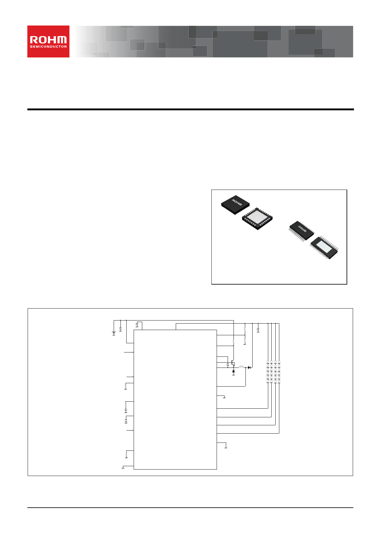
Application Circuit Diagram
CIN
VIN
(GND)
(GND)
(GND)
VREG
VCC
EN
VDISC
OVP
CS
BOOT
OUTH
SW
Vout
COUT
(DGND)
(DGND)
RRT
(GND)
SYNC
RT
RPC
CPC
(GND)
CSS
(GND)
COMP
SS
PWM
(DGND)
OUTL
BD81A04AMUV-M /
DGND
BD81A04AEFV-M
(DGND)
LED 1
LED 2
LED 3
LED 4
RISET
(GND)
(GND)
ISET
GND
SHDETEN
LEDEN 1
LEDEN 2
PGND
FAIL 1
(PGND)
FAIL 2
Figure 1. Buck-Boost Application Circuit
Product structure Silicon monolithic integrated circuit
www.rohm.com
© 2013 ROHM Co., Ltd. All rights reserved.
TSZ22111 15 001
This product has no designed protection against radioactive rays
1/34
TSZ02201-0G3G0C600010-1-2
4.Dec.2013 Rev.003
Free Datasheet http://www.datasheet4u.com/
1 page 
BD81A04AMUV-M BD81A04AEFV-M
Datasheet
Electrical Characteristics (VCC=12V, Ta = Tj = -40°C to +125°C *Unless otherwise specified.) - continued
Parameter
Symbol
Limits
Unit
Min Normal Max
Conditions
[UVLO]
UVLO Detection Voltage
VUVLO
3.2 3.5 3.8 V VCC : Sweep Down
UVLO Hysteresis Width
VUHYS
250 500 750 mV VCC : Sweep Up, VREG>3.5V
[LED Output]
LED Current Relative
Dispersion
LED Current Absolute
Dispersion
ISET Voltage
-3
-
+3
%
ILED=50mA, Ta=25°C
∆ILED1=(ILED/ILED_AVG-1)×100
ILED1
-5
-
+5
%
ILED=50mA, Ta=-40°C to +125°C
∆ILED1=(ILED/ILED_AVG-1)×100
ILED2
-3
-5
-
-
+3
%
ILED=50mA, Ta=25°C
∆ILED2=(ILED/50mA-1)×100
+5
%
ILED=50mA, Ta=-40°C to +125°C
∆ILED2=(ILED/50mA-1)×100
VISET
0.9 1.0 1.1 V RISET=100kΩ
PWM Minimum Pulse Width
TMIN
20
-
- μs FPWM=150Hz, ILED=100mA
PWM Maximum Duty
DMAX
-
- 100 % FPWM=150Hz, ILED=50mA
PWM Frequency
fPWM - - 20 kHz Duty=2%, ILED=50mA
[Protection Circuit]
LED Open Detection Voltage
VOPEN
0.2
0.3
0.4 V VLED= Sweep Down
LED Short Detection Voltage
VSHORT
4.2
4.5
4.8 V VLED= Sweep Up
LED Short Detection Latch
OFF Delay Time
tSHORT
70 100 130 ms RRT=27kΩ
PWM Latch OFF Delay Time
tPWM
70 100 130 ms RRT=27kΩ
SCP Latch OFF Delay Time
tSCP
70 100 130 ms RRT=27kΩ
[Logic Input]
Input High Voltage
VINH
2.1
-
VREG
V
Input Low Voltage
Input Current
VINL
GND
-
0.8 V
IIN
15
50
100
μA
VIN=5V(EN,SYNC,PWM,LEDEN1,
LEDEN2)
[FAIL Output (Open Drain)]
FAIL Low Voltage
VOL - 0.1 0.2 V IOL=0.1 A
www.rohm.com
© 2013 ROHM Co., Ltd. All rights reserved.
TSZ22111 15 001
5/34
TSZ02201-0G3G0C600010-1-2
4.Dec.2013 Rev.003
Free Datasheet http://www.datasheet4u.com/
5 Page 
BD81A04AMUV-M BD81A04AEFV-M
Datasheet
4. Self-Check Function
Table 2. Detection Condition of Each Protection Function and the Operation during Detection
Protection Function
Detection Condition
[Detection ]
[Release/ Cancellation]
Operation During Detection
UVLO
TSD
VCC<3.5V or VREG<2.0V
Tj>175°C
VCC >4.0V and VREG>3.5V
Tj<150°C
All Blocks Shuts down
(Except for VREG)
All Blocks Shuts down
(Except for VREG)
OVP
VOVP>2.0V
VOVP<1.45V
SS Pin Discharged
OCP
VCS≦VCC-0.6V
VCS>VCC-0.6V
SS Pin Discharged
SCP
VLED<0.3V
or
VOVP<0.57V
(100ms delay @300kHz)
EN or UVLO
Delay Counter starts and then
Latches Off all blocks
(Except for VREG)
LED Open Protection
VLED<0.3V
& VOVP>1.8V
EN or UVLO
Only the detected channel latches
OFF
LED Short Protection
VLED>4.5V
(100ms delay @300kHz)
EN or UVLO
Only the detected channel latches
OFF (After the counter starts )
Note1. The FAIL1 and FAIL2 output is reset when EN=Low ⇒ High or UVLO Detection ⇒ Release/ Cancel
EN Low or UVLO Detection are unfixed.
FFAAIILL11
FFAAIILL2
EN=Low or UVLO
EN=Low or UVLO
Figure 17. Protection Flag Output Block Diagram
The operating status of the built-in protection circuitry is propagated to FAIL1 and FAIL2 terminals (open-drain outputs).
FAIL1 becomes low when TSD, OVP, OCP, or SCP protection is engaged, whereas FAIL2 becomes low when open or
short LED is detected. If the FAIL terminal will not be used as flag output, please make the FAIL terminal open or connect it
to GND. But if the FAIL terminal will be used as a flag output, it is recommended to pull-up the FAIL1, 2 terminals to VREG
terminal.
(1) Under-Voltage Lock Out (UVLO)
The UVLO shuts down all the circuits other than VREG when VCC<3.5V(Typ) or VREG <2.0V(Typ)
(2) Thermal Shut Down (TSD)
The TSD shuts down all the circuits other than VREG when the Tj reaches 175°C (Typ), and releases when the Tj
becomes below 150°C (Typ).
(3) Over-Current Protection (OCP)
The OCP detects the current through the power-FET by monitoring the voltage of the high-side resistor, and activates
when the CS voltage becomes less than VCC-0.6V (Typ).
When the OCP is activated, the external capacitor of the SS terminal becomes discharged and the switching operation
of the DC/DC turns off.
(4) Over-Voltage Protection (OVP)
The output voltage of DC/DC is detected from the OVP terminal voltage, and the over-voltage protection will activate if
the OVP terminal voltage becomes greater than 2.0V (Typ). When OVP is activated, the external capacitor of the SS
terminal becomes discharged and the switching operation of the DC/DC turns off.
www.rohm.com
© 2013 ROHM Co., Ltd. All rights reserved.
TSZ22111 15 001
11/34
TSZ02201-0G3G0C600010-1-2
4.Dec.2013 Rev.003
Free Datasheet http://www.datasheet4u.com/
11 Page | ||
| Páginas | Total 30 Páginas | |
| PDF Descargar | [ Datasheet BD81A04AEFV-M.PDF ] | |
Hoja de datos destacado
| Número de pieza | Descripción | Fabricantes |
| BD81A04AEFV-M | 4ch White LED Driver | ROHM Semiconductor |
| Número de pieza | Descripción | Fabricantes |
| SLA6805M | High Voltage 3 phase Motor Driver IC. |
Sanken |
| SDC1742 | 12- and 14-Bit Hybrid Synchro / Resolver-to-Digital Converters. |
Analog Devices |
|
DataSheet.es es una pagina web que funciona como un repositorio de manuales o hoja de datos de muchos de los productos más populares, |
| DataSheet.es | 2020 | Privacy Policy | Contacto | Buscar |