|
|
|
PDF SKY77550 Data sheet ( Hoja de datos )
| Número de pieza | SKY77550 | |
| Descripción | Tx Quad-Band / Rx Dual-Band BiFET iPAC FEM | |
| Fabricantes | Skyworks Solutions | |
| Logotipo | ||
Hay una vista previa y un enlace de descarga de SKY77550 (archivo pdf) en la parte inferior de esta página. Total 19 Páginas | ||
|
No Preview Available !
PRELIMINARY DATA SHEET
SKY77550 Tx Quad-Band / Rx Dual-Band BiFET iPAC™ FEM for
GSM / GPRS (824-915 MHz and 1710-1910 MHz)
Applications
• Dual-band cellular handsets
encompassing
- Class 4 GSM850/900
- DCS1800/PCS1900
- Class 12 GPRS multi-slot
operation
Features
• High efficiency
- 42% (GSM850)
- 42% (GSM900)
- 42% (DCS1800
- 41% (PCS1900)
• Low transmit supply current
- 1.36 A (GSM850)
- 1.36 A (GSM900)
- 0.86 A (DCS1800)
- 0.88 A (PCS1900)
• Internal ICC sense resistor
for iPAC
• Closed loop iPAC
• 50 Ω matched Input/Output
• Tx–VCO-to-antenna and
antenna-to-Rx-SAW filter
RF interface
• RF switch affords high
linearity, low insertion loss,
and 0 V DC on Rx ports
• Small, low profile package
- 6 mm x 6 mm x 0.9 mm
- 28-pad configuration
Description
SKY77550 is a transmit and receive Front-End Module (FEM) with Integrated Power Amplifier Control
(iPAC™) designed in a low profile, compact form factor for dual-band cellular handsets comprising
GSM850/900 and DCS1800/PCS1900 operation. The SKY77550 offers a complete Transmit VCO-to-
Antenna and Antenna-to-Receive SAW filter solution. The FEM also supports Class 12 General Packet
Radio Service (GPRS) multi-slot operation.
The module consists of a GSM850/900 PA block and a DCS1800/PCS1900 PA block, impedance-
matching circuitry for 50 ohm input and output impedances, Tx harmonics filtering, high linearity / low
insertion loss RF switch, and a Power Amplifier Control (PAC) block with internal current sense
resistor. The two Heterojunction Bipolar Transistor (HBT) PA blocks, a BiFET PAC and switch control
circuit are fabricated onto a single Gallium Arsenide (GaAs) die. One PA block supports the
GSM850/900 bands and the other PA block supports the DCS1800/PCS1900 bands. Both PA blocks
share common power supply pads to distribute current. The output of each PA block and the outputs
to the two receive pads are connected to the antenna pad through an RF switch. The GaAs die, Switch
die and passive components are mounted on a multi-layer laminate substrate. The assembly is
encapsulated with plastic overmold.
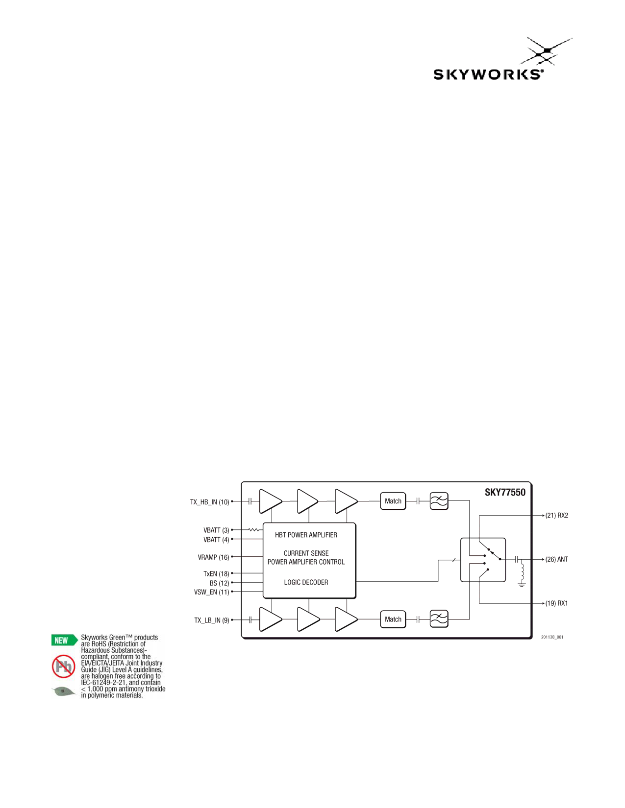
Band selection and control of transmit and receive are performed using four external control pads.
Refer to the block diagram in Figure 1 below. The band select pad, BS, selects GSM850, GSM900,
DCS, and PCS modes of operation. Transmit enable TxEN controls receive or transmit mode of the RF
switch (Tx = logic 1). Proper timing between transmit enable TxEN and Analog Power Control VRAMP
allows for high isolation between the antenna and Tx–VCO while the VCO is being tuned prior to the
transmit burst.
The SKY77550 is compatible with logic levels from 1.2 V to 2.9 V for BS, TxEN, and VSW_EN pads.
Figure 1. SKY77550 Functional Block Diagram
Skyworks Solutions, Inc. • Phone [781] 376-3000 • Fax [781] 376-3100 • [email protected] • www.skyworksinc.com
201138E • Skyworks Proprietary and Confidential Information • Products and Product Information are Subject to Change Without Notice. • September 8, 2010
1
Free Datasheet http://www.datasheet4u.com/
1 page 
SKY77550 Tx QUAD-BAND / Rx DUAL-BAND BiFET iPAC™ FEM for
GSM / GPRS (824-915 MHz and 1710-1910 MHz)
PRELIMINARY DATA SHEET
Table 5. SKY77550 Electrical Specifications1 (2 of 2)
[continued] GSM850 (Tx_LB) Mode (ƒ = 824 MHz to 849 MHz, –1 dBm ≤ PIN ≤ 5 dBm)
Parameter
Symbol
Test Condition
Coupling of GSM850/900 Tx Output (ƒ0) CGHI_Tx-Rx_ƒ0
to Rx5 Output pad4
Coupling of GSM850/900 Tx Output
(2ƒ0, 3ƒ0) to Rx5 Output pad4
CGHI_Tx-DCS_Rx
Spurious
Spur
Load Mismatch
Load
Rx Band Spurious
Rx_SPUR
Power Control Dynamic Range
Power Control
Variation
Control Level 5
PCDR
PCV
Control Level 6-15
Control Level 16-19
Power Control Slope
PCS
5 dBm ≤ POUT ≤ 33 dBm
5 dBm ≤ POUT ≤ 33 dBm
All combinations of the following parameters:
VRAMP = controlled2
PIN = min. to max.
3.1 V ≤ VCC ≤ 4.8 V
–20 °C ≤ TCASE ≤ +85 °C
Load VSWR = 12:1, all phase angles
All combinations of the following parameters:
VRAMP = controlled2
PIN = min. to max.
3.1 V ≤ VCC ≤ 4.8 V
–20 °C ≤ TCASE ≤ +85 °C
Load VSWR = 20:1, all phase angles
At ƒ0 + 20 MHz (869 MHz to 894 MHz)
RBW = 100 kHz
VCC = 3.5 V
TCASE = +25 °C
5 dBm ≤ POUT ≤ 33 dBm
At 1930 MHz to 1990 MHz
RBW = 100 kHz
VCC = 3.5 V
TCASE = +25 °C
5 dBm ≤ POUT ≤ 33 dBm
—
VBATT = 3.5 V
POUT = 33 dBm
TCASE = +25 °C
POUT = 33 dBm
VBATT = 3.5 V
13 dBm ≤ POUT ≤ 31 dBm
TCASE = +25 °C
13 dBm ≤ POUT ≤ 31 dBm
VBATT = 3.5 V
5 dBm ≤ POUT ≤ 11 dBm
TCASE = +25 °C
5 dBm ≤ POUT ≤ 11 dBm
5 dBm to 33 dBm
GSM850 RECEIVE (ƒ = 869 MHz to 894 MHz) Rx Mode
Minimum Typical Maximum Unit
⎯ –5
0 dBm
⎯ –45 –36 dBm
No parasitic oscillation > –35 dBm
No module damage or permanent
degradation
⎯ –84 –83 dBm
⎯ –101 –84
30 50
–1.5 ⎯
⎯ dB
1.5 dB
–2.0 ⎯
–2.5 ⎯
2.0
2.5
–3.5 ⎯
–4.5 ⎯
3.5
4.5
–5.5 ⎯
5.5
⎯ ⎯ 250 dB/V
Parameter
Symbol
Test Condition
Minimum Typical Maximum Units
Frequency Range
Insertion Loss, ANT to Rx5,3
VSWR ANT, Rx5,3
ƒ
IL_Rx5
ΓIN, ΓOUT
TCASE = +25 °C
—
—
869 ⎯ 894 MHz
⎯ 1.0 1.3 dB
⎯ 1.2:1 1.5:1
1 Unless specified otherwise:
TCASE = –20 °C to max. operating temperature (see Table 2); RL = 50 Ω; pulsed operation with pulse width ≤ 1154 μs and duty cycle ≤ 2:8; 3.1 V ≤ VCC ≤ 4.8 V.
2 VRAMP is calibrated to each PCL at TCASE = +25 °C, VBATT = 3.5 V, PIN = 3 dBm, 50 Ω load.
3 Terminate all unused RF ports with 50 Ω loads
4 Max VRAMP = VRAMP @ POUT =33 dBm, 50 Ω load, TCASE = +25 °C, VBATT = 3.5 V, PIN = 3 dBm
5 Rx1 and Rx2 are broadband receive ports and each supports the GSM850, GSM900, DCS, and PCS bands.
Skyworks Solutions, Inc. • Phone [781] 376-3000 • Fax [781] 376-3100 • [email protected] • www.skyworksinc.com
201138E • Skyworks Proprietary and Confidential Information • Products and Product Information are Subject to Change Without Notice. • September 8, 2010
5
Free Datasheet http://www.datasheet4u.com/
5 Page 
SKY77550 Tx QUAD-BAND / Rx DUAL-BAND BiFET iPAC™ FEM for
GSM / GPRS (824-915 MHz and 1710-1910 MHz)
PRELIMINARY DATA SHEET
Table 8. SKY77550 Electrical Specifications 1 (2 of 3)
[continued] PCS1900 (Tx_HB) Mode (ƒ = 1850 MHz to 1910 MHz, –1 dBm ≤ PIN ≤ 5 dBm)
Parameter
Symbol
Test Condition
Supply Current @ Rated Power
Supply Current @ Minimum Power
Harmonics
Mismatch Harmonics
Output Power
Input VSWR
Forward Isolation3
Coupling of PCS Tx Output to Receive
RF Output pad3
Spurious
ICC_31 dBm
VCC = 3.5 V
PIN = 3 dBm
POUT = 31 dBm
duty cycle 1:8
TCASE = +25 °C
ICC_28 dBm
VCC = 3.5 V
PIN = 3 dBm
POUT = 28 dBm
duty cycle 1:8
TCASE = +25 °C
ICC_0 dBm
VCC = 3.5 V
PIN = 3 dBm
POUT = 0 dBm
duty cycle 1:8
TCASE = +25 °C
2ƒ0 to 7ƒ0
BW = 3 MHz,
0 dBm ≤ POUT ≤ 31 dBm
VRAMP controlled2
2ƒ0, 3ƒ0
BW = 3 MHz
VRAMP = MAX VRAMP4
VBATT = 3.5 V
VSWR = 3:1 all phases
TCASE = +25 °C
POUT VCC = 3.5 V
TCASE = +25 °C
PIN = –1 dBm
POUT _MAX LOW VOLTAGE
VCC = 3.1 V
VRAMP = MAX VRAMP4
–20 °C ≤ TCASE ≤ +85 °C
PIN = –1 dBm
POUT _MAX HIGH VOLTAGE
VCC = 4.8 V
VRAMP = MAX VRAMP4
–20 °C ≤ TCASE ≤ +85 °C
PIN = –1 dBm
ΓIN 0 dBm POUT ≤ 31 dBm
VRAMP controlled2
POUT RX
PIN = 5 dBm
VRAMP ≤ 0.1 V
VSW_EN = VSW_EN _HIGH
TxEN = VTXEN_LOW
Rx2 Mode
POUT_ENABLED_TX
PIN = 5 dBm
VRAMP ≤ 0.1 V
VSW_EN = VSW_EN_HIGH
TxEN = VTXEN_HIGH
CPCS_Tx-Rx_ƒ0 0 dBm ≤ POUT ≤ 31 dBm
Spur All combinations of the following parameters:
VRAMP = controlled2
PIN = min. to max
3.1 V ≤ VCC ≤ 4.8 V
–20 °C ≤ TCASE ≤ +85 °C
Load VSWR = 12:1, all phase angles
Minimum Typical Maximum Units
⎯ 0.88 0.97 A
— 630 — mA
— 45 55 mA
⎯ –40 –33 dBm
–33 dBm
31.0 32.0
⎯ dBm
28.5 30.0
⎯
28.5 32.5
⎯
⎯ 1.5:1 2.5:1 ⎯
⎯ –60 –53 dBm
⎯ –35 –5
⎯0
5 dBm
No parasitic oscillation > –36 dBm
Skyworks Solutions, Inc. • Phone [781] 376-3000 • Fax [781] 376-3100 • [email protected] • www.skyworksinc.com
201138E • Skyworks Proprietary and Confidential Information • Products and Product Information are Subject to Change Without Notice. • September 8, 2010
11
Free Datasheet http://www.datasheet4u.com/
11 Page | ||
| Páginas | Total 19 Páginas | |
| PDF Descargar | [ Datasheet SKY77550.PDF ] | |
Hoja de datos destacado
| Número de pieza | Descripción | Fabricantes |
| SKY77550 | Tx Quad-Band / Rx Dual-Band BiFET iPAC FEM | Skyworks Solutions |
| SKY77552 | Quad-Band Tx / Dual-Band Rx iPAC FEM | Skyworks Solutions |
| SKY77554-21 | Tx Quad-Band / Rx Dual-Band BiFET iPAC FEM | Skyworks Solutions |
| SKY77555 | Tx-Rx FEM Based on CMOS PA | Skyworks Solutions |
| Número de pieza | Descripción | Fabricantes |
| SLA6805M | High Voltage 3 phase Motor Driver IC. |
Sanken |
| SDC1742 | 12- and 14-Bit Hybrid Synchro / Resolver-to-Digital Converters. |
Analog Devices |
|
DataSheet.es es una pagina web que funciona como un repositorio de manuales o hoja de datos de muchos de los productos más populares, |
| DataSheet.es | 2020 | Privacy Policy | Contacto | Buscar |