|
|
|
PDF NJW4822 Data sheet ( Hoja de datos )
| Número de pieza | NJW4822 | |
| Descripción | 1-Channel Low Side Switch | |
| Fabricantes | JRC | |
| Logotipo | ||
Hay una vista previa y un enlace de descarga de NJW4822 (archivo pdf) en la parte inferior de esta página. Total 14 Páginas | ||
|
No Preview Available !
NJW4822
1-Channel Low Side Switch
GENERAL DESCRIPTION
The NJW4822 is the single low-side switch that can supply 0.2A.
The active clamp, overcurrent, error flag output and thermal
shutdown are built in with Nch MOS FET.
It can be controlled by a logic signal (3V/5V) directly. Especially, the
NJW4822 is suitable for various Sensors output block as NPN
type. The FLT logic has two versions: Active-high (A-ver) and
Active-low (B-ver).
Also, The NJW4822 is a complementary product to the NJW4832.
FEATURES
Drain-Source Voltage
43V
Drain Current
0.2A
Corresponding with Logic Voltage Operation: 3V/5V
Low On-Resistance
1.1 (typ.) (VIN=5V)
Low Consumption Current
1.3 (typ.) (VIN=3.3V)
160A (typ.) (VIN=5V)
Active Clamp Circuit
135A (typ.) (VIN=3.3V)
Over Current Protection
Thermal Shutdown
Package Outline
DFN6-H1 (ESON6-H1)
PACKAGE OUTLINE
NJW4822KH1
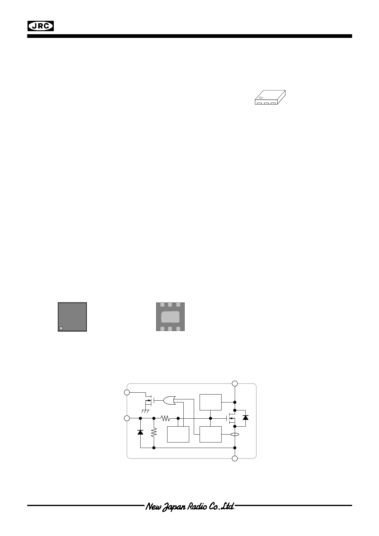
PIN CONFIGURATION
6 54
123
(Top View)
1. NC
2. NC
3. DRAIN
4. IN
5. SOURCE
6. FLT
BLOCK DIAGRAM
1 23
654
(Bottom View)
Exposed PAD on backside
connect to GND.
DRAIN
FLT
Active
Clamp
IN
Thermal
Shut Down
Over
Current
Protection
SOURCE
Ver.2015-06-22
-1-
1 page 
TIMING CHART
ON, OFF Switching Time (VIN=0 to 5V, VDS=13V, ID=0.2A)
90%
IN
10%
DRAIN
10%
90%
tON tOFF
FLT delay at OCP detection and OCP release (VIN=0 to 5V, FLT=Pull-up)
[A-version: Active-high]
NJW4822
[B-version: Active-low]
Ver.2015-06-22
-5-
5 Page 
CHARACTERISTICS
Turn-on Time vs. Ambient Temperature
20
18 VIN=3.3V
VIN=5.0V
16
14
12
10
8
6
4
2
0
-50
-25 0 25 50 75 100 125 150
Ambient Temperature [ºC]
FLT delay Time at OCP Detection
vs. Ambient Temperature
1
0.9
0.8
0.7
0.6
0.5
0.4
0.3
0.2
0.1
0
-50
VIN=3.3V
VIN=5.0V
-25 0 25 50 75 100 125 150
Ambient Temperature [ºC]
FLT Pin Low Level Output Voltage
vs. Ambient Temperature
0.3
0.25
0.2
0.15
0.1
0.05
0
-50
-25 0 25 50 75 100 125
Ambient Temperature [ºC]
150
Ver.2015-06-22
NJW4822
Turn-off Time vs. Ambient Temperature
20
18 VIN=3.3V
VIN=5.0V
16
14
12
10
8
6
4
2
0
-50
-25 0 25 50 75 100 125
Ambient Temperature [ºC]
150
FLT delay Time at OCP Release
vs. Ambient Temperature
1
0.9 VIN=3.3V
VIN=5.0V
0.8
0.7
0.6
0.5
0.4
0.3
0.2
0.1
0
-50
-25 0 25 50 75 100 125 150
Ambient Temperature [ºC]
200
180
160
140
120
100
80
60
40
20
0
2
TSD Detection/Release Temperature
vs. Input Voltage
Detection Temp
Release Temp
2.5 3 3.5 4 4.5 5 5.5 6
Input Voltage [V]
- 11 -
11 Page | ||
| Páginas | Total 14 Páginas | |
| PDF Descargar | [ Datasheet NJW4822.PDF ] | |
Hoja de datos destacado
| Número de pieza | Descripción | Fabricantes |
| NJW4820 | 35V / 500mA Low Side Switch | New Japan Radio |
| NJW4822 | 1-Channel Low Side Switch | JRC |
| Número de pieza | Descripción | Fabricantes |
| SLA6805M | High Voltage 3 phase Motor Driver IC. |
Sanken |
| SDC1742 | 12- and 14-Bit Hybrid Synchro / Resolver-to-Digital Converters. |
Analog Devices |
|
DataSheet.es es una pagina web que funciona como un repositorio de manuales o hoja de datos de muchos de los productos más populares, |
| DataSheet.es | 2020 | Privacy Policy | Contacto | Buscar |