|
|
|
PDF SH69P43 Data sheet ( Hoja de datos )
| Número de pieza | SH69P43 | |
| Descripción | OTP 4-Bit Microcontroller | |
| Fabricantes | Sino Wealth | |
| Logotipo | ||
Hay una vista previa y un enlace de descarga de SH69P43 (archivo pdf) en la parte inferior de esta página. Total 30 Páginas | ||
|
No Preview Available !
SH69P43
OTP 4-bit Microcontroller with SAR 8-bit A/D Converter
Features
The SH6610D-based single-chip 4-bit microcontroller
with 8-bit SAR A/D converter
OTP ROM: 3072 X 16 bits
RAM: 192 X 4 bits
- System register: 48 X 4 bits
- Data memory: 144 X 4 bits
Operation voltage:
- fOSC = 400KHz - 4MHz, VDD = 2.4V - 5.5V
- fOSC = 8MHz, VDD = 4.5V - 5.5V
24 CMOS bi-directional I/O pins
Built in pull-up for I/O port
Two 8-bit auto re-load timers/counters, One can switch
to external clock source
8-level subroutine nesting (including interrupts)
Powerful interrupt sources:
- A/D interrupt
- Internal interrupt (Timer1, Timer0)
- External interrupts: Port A - D (Falling edge)
Oscillator: (OTP option)
- Crystal oscillator: 32768Hz, 400KHz - 8MHz
- Ceramic resonator: 400K - 8MHz
- External ROSC RC oscillator: 400K - 8MHz
- Internal ROSC RC oscillator: 4MHz
- External clock: 30K - 8MHz
Instruction cycle time:
- 4/32.768KHz (≈ 122µs) for 32.768KHz
- 4/8MHz (= 0.5µs) for 8MHz at VDD = 5.0V
8 channels 8-bit resolution A/D converters
2 channels 10-bit PWM outputs
Warm-up timer for power on reset
Low voltage reset function (LVR)
Internal reliable reset circuit
Built-in watchdog timer
Two low power operation modes: HALT and STOP
OTP type/Code protection
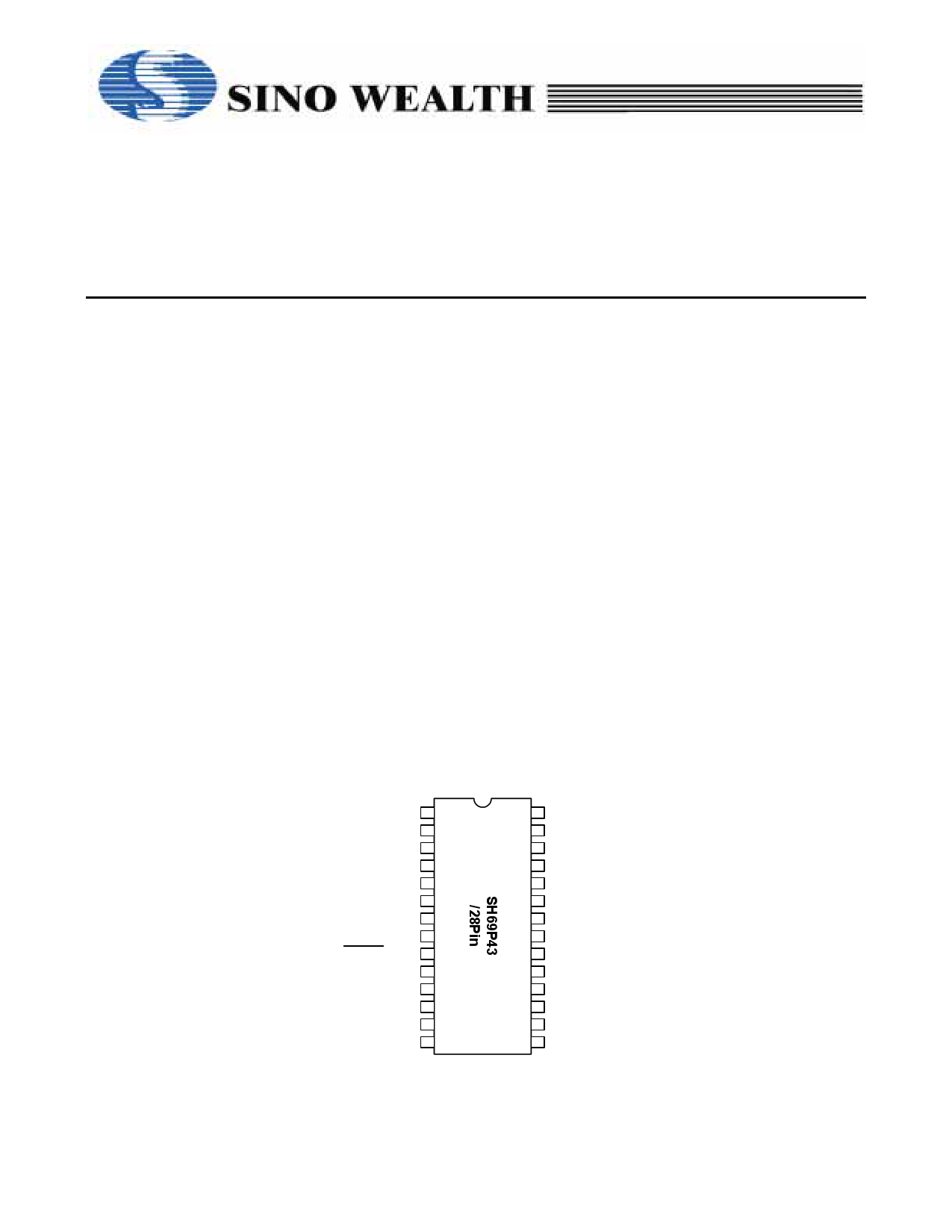
28-pin SOP/SKINNY package
General Description
The SH69P43 is an advanced CMOS 4-bit microcontroller. It provides the following standard features: 3K words of OTPROM,
192 nibbles of RAM, 8-bit timer/counter, 8-bit A/D converter, 10-bit high speed PWM output, on-chip oscillator clock circuitry,
on-chip watchdog timer, low voltage reset function and supports power saving modes to reduce power consumption.
Pin Configuration
PORTF.2
PORTF.3
PORTE.2
PORTE.3
PORTD.2
PORTD.3/PWM1
PORTC.2/PWM0
PORTC.3/T0
RESET /VPP
GND
PORTA.0/AN0/SDA
PORTA.1/AN1
PORTA.2/AN2
PORTA.3/AN3
1
2
3
4
5
6
7
8
9
10
11
12
13
14
28 PORTF.1
27 PORTF.0
26 PORTE.1
25 PORTE.0
24 PORTD.1
23 PORTD.0
22 PORTC.1/VREF
21 OSCO/PORTC.0
20 OSCI/SCK
19 VDD
18 PORTB.3/AN7
17 PORTB.2/AN6
16 PORTB.1/AN5
15 PORTB.0/AN4
1 V2.6
Free Datasheet http://www.datasheet4u.net/
1 page 
SH69P43
Functional Description
1. CPU
The CPU contains the following functional blocks: Program
Counter (PC), Arithmetic Logic Unit (ALU), Carry Flag (CY),
Accumulator, Table Branch Register, Data Pointer (INX,
DPH, DPM, and DPL) and Stacks.
1.1. PC
The PC is used for ROM addressing consisting of 12-bits:
Page Register (PC11), and Ripple Carry Counter (PC10,
PC9, PC8, PC7, PC6, PC5, PC4, PC3, PC2, PC1, PC0).
The program counter is loaded with data corresponding to
each instruction. The unconditional jump instruction (JMP)
can be set at 1-bit page register for higher than 2K.
The program counter can only have 4K program ROM
address. (Refer to the ROM description).
1.2. ALU and CY
The ALU performs arithmetic and logic operations. The ALU
provides the following functions:
Binary addition/subtraction (ADC, SBC, ADD, SUB, ADI, SBI)
Decimal adjustments for addition/subtraction (DAA, DAS)
Logic operations (AND, EOR, OR, ANDIM, EORIM, ORIM)
Decisions (BA0, BA1, BA2, BA3, BAZ, BC)
Logic Shift (SHR)
The Carry Flag (CY) holds the ALU overflow that the
arithmetic operation generates. During an interrupt service
or call instruction, the carry flag is pushed into the stack and
recovered from the stack by the RTNI instruction. It is
unaffected by the RTNW instruction.
1.3. Accumulator
The accumulator is a 4-bit register holding the results of the
arithmetic logic unit. In conjunction with the ALU, data is
transferred between the accumulator and system register,
or data memory can be performed.
1.4. Table Branch Register (TBR)
Table Data can be stored in program memory and
referenced by using Table Branch (TJMP) and Return
Constant (RTNW) instructions. The Table Branch
Register (TBR) and Accumulator (A) is placed by an
offset address in program ROM. TJMP instruction branch
into address ((PC11 - PC8) X (28) + (TBR, A)). The
address is determined by RTNW to return the look-up
value into (TBR, A). ROM code bit7-bit4 is placed into
TBR and bit3-bit0 into A.
1.5. Data Pointer
The Data Pointer can indirectly address data memory.
Pointer address located in register DPH (3-bits), DPM
(3-bits) and DPL (4-bits). The addressing range can have
3FFH locations. Pseudo index address (INX) is used to
read or write Data memory, and RAM address bit9 - bit0
comes from DPH, DPM and DPL.
1.6. Stack
The stack is a group of registers used to save the contents
of CY & PC (11-0) sequentially with each subroutine call or
interrupt. The MSB is saved for CY and organized into 13
bits X 8 levels. The stack is operated on a first-in, last-out
basis and returned sequentially to the PC with the return
instructions (RTNI/RTNW).
Note:
The stack nesting includes both subroutine calls and
interrupts requests. The maximum allowed for subroutine
calls and interrupts are 8 levels. If the number of calls and
interrupt requests exceeds 8, then the bottom of stack will
be shifted out, that program execution may enter an
abnormal state.
2. RAM
Built-in RAM containing general-purpose data memory and system register.
2.1. RAM Addressing
Data memory and system register can be accessed in one instruction by direct addressing. The memory allocation map is
given below:
$000 - $02F: System register and I/O
$030 - $0BF: Data memory (144 X 4 bits)
2.2. Data Memory
Data memory is organized as 144 X 4 bits ($030 - $0BF). Because of its static nature, the RAM can keep the data after the
CPU enters STOP or HALT.
5
Free Datasheet http://www.datasheet4u.net/
5 Page 
SH69P43
6. I/O Port
The MCU provides 24 programmable bi-directional I/O ports. Each I/O port contains pull-up MOS controllable by the program.
The pull-up MOS is controlled by the port data registers (PDR) of each port also when the Port is input port (Write “1” to turn
on the pull-up MOS and “0” to turn off the pull-up MOS). So, the pull-up MOS can be turned on and off individually. The port
control register (PCR) controls the I/O port’s direction (input or output). When Ports A, B, C, D are in the digital input direction,
they can have active port interrupt by the falling edge (if the port interrupt is enabled).
- PortA.0 - 3 can be shared with ADC AN0 - 3 input channel,
- PortB.0 - 3 can be shared with ADC AN4 - 7 input channel,
- PortC.0 can be shared with OSCO pin, (if used External clock or RC oscillator, OTP option)
- PortC.1 can be shared with ADC reference voltage input,
- PortC.2 can be shared with PWM0 output,
- PortC.3 can be shared with T0 input,
- PortD.3 can be shared with PWM1 output.
System Register $08 - $0D: Port Data Register (PDR)
Address
$08
$09
$0A
$0B
$0C
$0D
Bit 3
PA.3
PB.3
PC.3
PD.3
PE.3
PF.3
Bit 2
PA.2
PB.2
PC.2
PD.2
PE.2
PF.2
Bit 1
PA.1
PB.1
PC.1
PD.1
PE.1
PF.1
Bit 0
PA.0
PB.0
PC.0
PD.0
PE.0
PF.0
R/W
R/W PORTA
R/W PORTB
R/W PORTC
R/W PORTD
R/W PORTE
R/W PORTF
Remarks
System Register $18 - $1D: Port Control Register (PCR)
Address
$18
$19
$1A
$1B
$1C
$1D
Bit 3
PACR.3
PBCR.3
PCCR.3
PDCR.3
PECR.3
PFCR.3
Bit 2
PACR.2
PBCR.2
PCCR.2
PDCR.2
PECR.2
PFCR.2
Bit 1
PACR.1
PBCR.1
PCCR.1
PDCR.1
PECR.1
PFCR.1
Bit 0
PACR.0
PBCR.0
PCCR.0
PDCR.0
PECR.0
PFCR.0
R/W Remarks
R/W PORTA input/output control
R/W PORTB input/output control
R/W PORTC input/output control
R/W PORTD input/output control
R/W PORTE input/output control
R/W PORTF input/output control
I/O control register:
PA (/B/C/D/E/F) CR.n, (n = 0, 1, 2, 3)
0: Set I/O as an input direction. (Default)
1: Set I/O as an output direction.
DATA
WRITE
D PDR Q
CK Q
RESET
RESET
DATA IN
READ
CONTROL
WRITE
D PCR Q
CK Q
RESET
RESET
AND
OR
VDD
Pull up MOS
VDD
I/O PIN
GND
11
Free Datasheet http://www.datasheet4u.net/
11 Page | ||
| Páginas | Total 30 Páginas | |
| PDF Descargar | [ Datasheet SH69P43.PDF ] | |
Hoja de datos destacado
| Número de pieza | Descripción | Fabricantes |
| SH69P42 | OTP 4-Bit Microcontroller | Sino Wealth Microelectronic |
| SH69P43 | OTP 4-Bit Microcontroller | Sino Wealth |
| SH69P48 | OTP 4K 4-bit Micro-controller | Sino Wealth |
| SH69P48A | OTP 4K 4-bit Micro-controller | Sino Wealth |
| Número de pieza | Descripción | Fabricantes |
| SLA6805M | High Voltage 3 phase Motor Driver IC. |
Sanken |
| SDC1742 | 12- and 14-Bit Hybrid Synchro / Resolver-to-Digital Converters. |
Analog Devices |
|
DataSheet.es es una pagina web que funciona como un repositorio de manuales o hoja de datos de muchos de los productos más populares, |
| DataSheet.es | 2020 | Privacy Policy | Contacto | Buscar |